Transcription
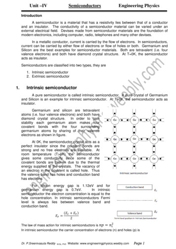
Unit –IVSemiconductorsEngineering PhysicsIntroductionA semiconductor is a material that has a resistivity lies between that of a conductorand an insulator. The conductivity of a semiconductor material can be varied under anexternal electrical field. Devises made from semiconductor materials are the foundation ofmodern electronics, including computer, radio, telephones and many other devises.In a metallic conductor, current is carried by the flow of electrons. In semiconductors,current can be carried by either flow of electrons or flow of holes or both. Germanium andSilicon are the best examples for semiconductor materials. Both are tetravalent (i.e. fourvalence electrons) and both have diamond crystal structure. At T 0K, the semiconductoracts as insulator.Semiconductors are classified into two types, they are1. Intrinsic semiconductor2. Extrinsic semiconductor1.Intrinsic semiconductorA pure semiconductor is called intrinsic semiconductor. A pure crystal of Germaniumand Silicon is an example for intrinsic semiconductor. At T 0K, the semiconductor acts asinsulator.Germanium and silicon are tetravalentatoms (i.e. four valence electrons) and both havediamond crystal structure.In order to gainstability each germanium atom makes fourcovalent bonds with the four surroundinggermanium atoms by sharing of their valenceelectrons as shown in figure.At 0K, the semiconductor crystal acts as aperfect insulator since the covalent bonds arestrong and no free electrons are available. Atroom temperature (T 0K) the semiconductorgives some conductivity since some of thecovalent bonds are broken due to the thermalenergy supplied to the crystals. The vacancy ofan electron in the covalent is called hole. Thusthe valence band has holes and conduction bandhas electronsFor silicon energy gap is 1.12eV and forgermanium energy gap is 0.7eV.In intrinsicsemiconductor the electron concentration is equal to thehole concentration. In intrinsic semiconductors Fermilevel is always lies between valence band andconduction band. 2The law of mass action for intrinsic semiconductors is In intrinsic semiconductor the carrier concentration of electrons (n) and holes (p) isDr. P.Sreenivasula ReddyM.Sc, PhDWebsite: www.engineeringphysics.weebly.comPage 1
Unit –IV SemiconductorsEngineering Physics 2. Intrinsic carrier concentrationIn intrinsic semiconductorn pHence n p ni is called intrinsic carrier concentration. . . Where EC EV E g is the forbidden gap. !/ The above equation shows the intrinsic carrier concentration.3. Fermi level in intrinsic semiconductorIn intrinsic semiconductor n p e( 2 E F ( EC EV )kTTaking logarithms on both sides Nlog V NC 2 EF ( EC EV ) kT NKT log V NC 2 EF ( EC EV ) N2 EF ( EC EV ) KT log V NCDr. P.Sreenivasula ReddyM.Sc, PhDQ log e e x x Website: www.engineeringphysics.weebly.comPage 2
Unit –IVSemiconductorsEF Engineering Physics N ( E EC )KTlog c V22 NV If we assume that N C NVEF EC EV2Thus the Fermi level in intrinsic semiconductor is always lies between the valence band andconduction band.4. Intrinsic conductivityIn semiconductor, the electrons and holes will participate in electrical conductivity. Toobtain an expression for electrical conductivity, we consider a rectangular bar of intrinsicsemiconductor connected to a battery is shown in figure. When an electric field is appliedalong X-axis, the electrons move along negative X-axis and holes move along X-axis. Due tofield, the charge carriers attain some constant velocity. This constant velocity is called driftvelocity, represented by # .# % (1)Let n be the concentration of electrons in semiconductor. Then the current density due to anelectron is&' # (2)From equations (1) and (2) we get&' %' Similarly the, current density of hole is&( %( (3)The total electric current density passing through the semiconductor is the sum of electroncurrent density &' and hole current density &( .&)*) , &' &(&)*) , %' %( &)*) , %' %( (4)From ohm’s law& - (5)From equation (4) and (5)- %' %( (5)Equation (5) represents the total electrical conductivity in semiconductorIn intrinsic semiconductor - %' %( (7)Intrinsic carrier concentration!/ . Substituting equation (8) in equation (7) we get- %' %( / 0 - 6 1/22 3245(8)2 3 245!/Where 6 % %7 Dr. P.Sreenivasula ReddyM.Sc, PhDWebsite: www.engineeringphysics.weebly.comPage 3
Unit –IVSemiconductorsEngineering Physics5. Energy gap of a semiconductorThe energy gap between valence band and conduction band is called energy band gap orforbidden band gap.In intrinsic semiconductor the resistivity of a semiconductor can be written as8 !9 ! ; : .' . @A8 ?BC DETaking ln on both side@Aln 8 ln ?BC DE ln 6The energy gap of a semiconductor can be calculated by measuring slope of the!graph ln 8 0H . I J K 24 5 I J6. Extrinsic semiconductorAn impure semiconductor is called as extrinsic semiconductor. Depending upon onthe type of impurity added to the intrinsic semiconductor, these are two types.n- type extrinsic semiconductorp- type extrinsic semiconductorn- type extrinsic semiconductor:Intrinsic semiconductor is doped with v groupelements such as phosphorus (P), arsenic (As), andantimony (Sb), n – type semiconductor is formed. Vgroup elements contain five valence electrons.When v group element is added to puresemiconductor, four valence electrons of impurityatoms makes four covalent bonds with the foursurrounded intrinsic atoms and fifth electron isloosely bounded with the parent atom. When itreceived a small amount of energy, the fifth valenceelectron is excited into conduction band formacceptor level. As a result the donor levels getionized.Dr. P.Sreenivasula ReddyM.Sc, PhDWebsite: www.engineeringphysics.weebly.comPage 4
Unit –IVSemiconductorsEngineering PhysicsThese free electrons are responsible for electrical conduction. At higher temperature theelectron hole pairs are created by breaking the covalent bond i.e. electron excited into theconduction band leaving the holes in the valence band. As a result, the concentrations ofelectrons are greater than holes. Hence electrons are the majority charge carriers and holesare minority charge carriers. The v group impurity atoms are also called donor impurityatoms.In n-type semiconductors, the Fermi is always lies between conduction level anddonor level at lower temperatures but at higher temperatures the Fermi level moves towardsthe intrinsic Fermi level. N 2 KT log C 2 ND p- Type extrinsic semiconductor:Intrinsic semiconductor is doped with IIIgroup elements such as Aluminium (Al), gallium(Ga), indium (In) p – type semiconductor is formed.III group elements contain three valence electrons.When III group element is added to puresemiconductor, three valence electrons of impurityatoms makes three covalent bonds with the threesurrounded intrinsic atoms and one bond is leftover with the deficiency of one electron. When thetemperature is raised ( 0K) the electrons from thevalence band try to occupy the acceptor and it getsionized creating the hole in the valence band.These holes are responsible for electricalconduction. At higher temperature the electron hole pairs are created by breaking thecovalent bond i.e. electron excited into the conduction band leaving the holes in the valenceband. As a result, the concentrations of holes are greater than electrons. Hence holes are themajority charge carriers and electrons are minority charge carriers. The III group impurityatoms are also called acceptor Impurity atoms.In p-type semiconductor, the Fermi level is always lies between valence level andacceptor level at lower temperatures but at higher temperatures the Fermi level movestowards the intrinsic Fermi level. Dr. P.Sreenivasula ReddyM.Sc, PhD N KT log V 2 NA Website: www.engineeringphysics.weebly.comPage 5
Unit –IVSemiconductorsEngineering Physics7. Law of mass actionAccording to law of mass action “the product of majority and minority charge carrierconcentration at a particular temperature is equal to the square of intrinsic carrierconcentration at that particular temperature.”L L In intrinsic semiconductor, expressions for the electron and hole concentrations Eare In intrinsic semiconductor electron concentration is equal to the hole concentration. For n-type semiconductor, the law of mass relation can be written asN N (1)For p-type semiconductor, the law of mass relation can be written as (2)From equations (1) and (2) we observe that, the product of majority and minority chargecarrier concentration at a particular temperature is equal to the square of intrinsic carrierconcentration at that particular temperature.L L8. Direct and indirect band gap semiconductorsDirect band gap semiconductorIn direct gap semiconductors the banddiagram between energy and wave vector (E-Kcurve) is shown in figure.In direct band gap semiconductors the maximumof the valance band and minimum of theconduction band present at the same of k asshown in figure.In direct band gap semiconductors, when anelectron recombines with the hole, emits theirenergy in terms of light.Dr. P.Sreenivasula ReddyM.Sc, PhDWebsite: www.engineeringphysics.weebly.comPage 6
Unit –IVSemiconductorsEngineering PhysicsLife time (recombination time) of charge carriers is very less.Compound semiconductors like GaAs and InP are examples for direct band gapsemiconductors.Band gap of InP 1.35eV and, GaAs 1.4eV. Direct band gap semiconductor is used tofabricate LEDs and laser diodes.Indirect band gap semiconductorIn in-direct gap semiconductors the banddiagram between energy and wave vector(E-K curve) is shown in figure.In indirect band gap semiconductors, themaximum of the valance band andminimum of the conduction band present atthe different values of k as shown in figure.In Indirect band gap semiconductors, whenan electron recombines with the hole, emitstheir energy in terms of heat.So indirect band gap semiconductors are not used in the preparation of semiconductor laser.Life time (recombination time) of charge carriers is more.Elemental semiconductors like germanium and silicon are examples for in-direct gapsemiconductors.Band gap of Ge 0.7eV and Si 1.12eV. .fabricate diodes and transistors.Indirect band gap semiconductor is used to9. Differences between direct and indirect band gap semiconductorDirect band gap semiconductors1. In direct gap semiconductors theband diagram between energy andwave vectoris shown inEConduction BandfigureIndirect gap semiconductors1. In in-direct gap semiconductors theband diagram between energy andwave vector is shown in figureE KEgkkValence BandValance BandDirect band gap semiconductorIndirect band gap semiconductor2. In direct band gap semiconductorsthe maximum of the valance bandand minimum of the conduction bandpresent at the same of kDr. P.Sreenivasula ReddyConduction BandM.Sc, PhD2. In in-direct band gap semiconductorsthe maximum of the valance bandand minimum of the conduction bandpresent at the different values of kWebsite: www.engineeringphysics.weebly.comPage 7
Unit –IVSemiconductorsEngineering Physics3. In direct band gap semiconductors,when an electron recombines withthe hole, it emits their energy interms of light.4. Life time(recombination time) ofcharge carriers is very less.3. In direct band gap semiconductors,when an electron recombines withthe hole, it emits their energy interms of heat.4. Life time (recombination time) ofcharge carriers is more.5. These are mostly formcompound semiconductors.5. These are mostly form the elementalsemiconductors.the6. Examples: InP, GaAs.6. Examples: Germanium and silicon.7. Band gap of InP 1.35eV and ,GaAs 1.42eV7. Band gapSi 1.12eV8. Direct band gap semiconductors areused to fabricate LEDs and laserdiodes8. Indirect band gap semiconductorsare used to fabricate diodes andtransistorsofGe 0.7eVand10. Drift current and diffusion currentsIn case of semiconductors we observe two kinds of currents.I.II.Drift currentDiffusion currentDrift currentDefinition:- The flow of electric current due to the motion of charge carriers under theinfluence of external electric field is called drift current.When an electric field E is applied across a semiconductor material, the chargecarriers attain a drift velocity # .So drift velocity # µ . (1)The relation between current density J and drift velocity# . is& O# Where N is the carrier concentrationq is the charge of electron or holeFrom equations (1) and (2), we get(2)& P Q) Oµ µ is the mobility of charge carrier.The above equation shows the general expression for drift current density.Drift current density due to electrons is P Q)&' µR Where is the electrons carrier concentration andµR is the mobility of electronsDrift current density due to holes is P Q)&(Dr. P.Sreenivasula ReddyM.Sc, PhD µS Website: www.engineeringphysics.weebly.comPage 8
Unit –IVSemiconductorsEngineering PhysicsWhere is the carrier concentration of holes.µS is the mobility of holesT Total drift current density& P Q) UVUWX &' P Q) &( P Q) µY µS nµR pµS Diffusion currentDefinition:The flow of electric current due to the motion of charge carriers under concentrationgradient is called diffusion currentOrThe motion of charge carriers from the region of higher concentration to lowerconcentration leads to a current called diffusion current.Let be the excess electron concentration. Then according to Fick’s law, the rate ofdiffusion of charge carriers is proportional to concentration gradientRate of diffusion of charge 2\ ] ?2\ ] \]E\]\ ] 2\]Where D is the diffusion coefficient of charge carriersThe negative sign indicates decrease of N with increase of xSo, the diffusion current density & QQ is&abccd O e2f gf 2Of f Where q is the charge of the charge carrierDiffusion current density due to holes is& ( QQ 2 . (f fJDiffusion current density due to electrons is& ' QQ . 'f fJ and – are the charges of holes and electrons respectively.The expression for total diffusion current density is& Q UVUWX & ( QQ & ' QQ & QQ UVUWX 2 . (f f . 'fJfJThe expression for total current density due to holes is&( UVUWX & ( P Q) & ( QQ &( UVUWX µS 2 . (f fJThe expression for total current density due to electrons is&' UVUWX & ' P Q) & ' QQ &' UVUWX µR . 'Dr. P.Sreenivasula ReddyM.Sc, PhDf fJWebsite: www.engineeringphysics.weebly.comPage 9
Unit –IVSemiconductorsEngineering Physics11. Einstein relationThe relation between mobility and diffusion coefficient of charge carriers in asemiconductors is known as Einstein relation.At equilibrium conducting condition, the drift and diffusion currents must be equal andopposite in direction. Any disturbance in equilibrium leads to diffusion of charge carriersresulting in diffusion current which creates an internal electric field. This field causes thedrifting of charge carriers resulting in a drift current. Then at equilibrium the drift and diffusioncurrents balance each other.Let bet he excess electrons concentration of a semiconductors. Then µR . '\ N (1)\JThe force on excess electrons restoring equilibrium is equal to the product of excess chargeand the electric field, i.e.,i (2)From equations (1) and (2)j \ N i µkl(3)\JFrom kinetic theory of gasses, the force on charge carriers can be written asi 45\ N (4)\JForm equations (3) and (4)' 45 µReSimilarly for holes we get( 45 µSe' ( µR µS( ' %( %'This is called Einstein relation.12. Hall EffectStatement:Hall Effect was discovered by E.H hall in 1879. When a magnetic field is appliedperpendicular to the current carrying semiconductor, a potential difference of electric field isdeveloped between two points on the opposite sides of the semiconductor in directionperpendicular to the both current and magnetic field. This phenomenon is known as Halleffect.Let a current b is passed in the conductor along X axis and a magnetic field B isapplied along Y axis. Due to the magnetic field, the charge carriers experience a force Fperpendicular to X-Y plane i.e., along Z axis. The direction of force is given by the Flemingsleft hand rule. Due to the displacement of the charge carriers, some transverse field knownas hall electric field n is developed across the two faces O# oHall electric deflecting force O nMagnetic deflection forceDr. P.Sreenivasula ReddyM.Sc, PhDWebsite: www.engineeringphysics.weebly.com(1)(2)Page 10
Unit –IVSemiconductorsEngineering PhysicsAt the equilibrium O# o O n n # oWe know drift velocity # (3)p(4)]qWhere N is the number of charge carriers per unit volume.So from equations (3) and (4) n p]qo(5)Then the hall voltage 0n at the equilibrium is n ar(6)Hall coefficient (st )The ratio of the hall electric field to the product of current density and magnetic induction isknown as Hall coefficient. un r(7)p:Substitute the value of n from equation (5) in equation (7).We get 1un r Op:Hall coefficient for n-type semiconductors isun 21 Hb / cVv X /UvV1 Hb / cVv 7VX H O W a O 2 W a Hall coefficient for n-type semiconductors isun The hall coefficient is negative when the charge carriers are electrons and positive when thecharge carriers are holes.Applications of Hall Effect1. Hall Effect gives the information about the sign of the charge carriers.2. Hall Effect can be used to measure the drift velocity of the charge carriers. # pNq3. Strong magnetic fields can be measured by using Hall Effect.4. The mobility of the charge carrier can be measured by the conductivity of the materialand Hall coefficient.5. Hall Effect can be used to measure the number of charge carriers per unit volume.Dr. P.Sreenivasula ReddyM.Sc, PhDWebsite: www.engineeringphysics.weebly.comPage 11
Unit –IVSemiconductorsEngineering Physics13. Photo diodeSilicon photo diode is a light sensitive device. It is also called as photo detector. Photo diodeconverts light signals into electrical signals. It is always operated in reverse biased condition.SymbolConstructionThe diode is made of semiconductor pnjunction kept in a sealed plastic casing. The cover isso designed that the light rays are allowed to fall onone surface of junction and the remaining sides ofthe casing are painted to restrict the penetration oflight rays. A lens permits light to fall on the junction.WorkingWhen light falls on the reverse biased p-n photo diode junction, hole-electron pairs createdby breaking of covalent bondings. The magnitude of photo current depends on the numberof charge carriers generated and on the light falling of diode element. The current is alsoaffected by the frequency of the light falling on the diode element. The magnitude of currentunder large reversed bias is given byw wx wy ?1 2 {z EWhere wx short circuit current which is proportional to the light intensitywy Reverse saturation current0 Voltage across the diode0 Volt equilent of temperature Parameter, 1 for Ge, 2 for SiCharacteristicsThe Characteristics of photo diode are shown infigure. The reverse current increases in directproportion to the level of light. Even no light isapplied, there is minimum reverse lekage currentcalled dark current, flowing through the diode.Germanium has higher dark current than silicon.ApplicationsPhoto diodes are used asLight detectors,Demodulators,Encoders.Optical communication systemHigh speed counting and switching circuits.Dr. P.Sreenivasula ReddyM.Sc, PhDWebsite: www.engineeringphysics.weebly.comPage 12
Unit –IVSemiconductorsEngineering Physics14. LIGHT EMITTING DIODE (LED)Light emitting diode is a pn junction device. It is always operated in forward biasedcondition. LED converts electrical energy into light energy. In the fabrication of LED’s directband gap semiconductors like GaP, GaAsP are used. In direct band gap semiconductorsmost of the energy is emitted in the form of light when hole and electron recombination takesplace.SymbolConstructionThe basic structure and of anLED is shown in figure. In LED, an Ntype layer is grown on a substrate and ap type is deposited on it by diffusion. Ametal (gold) coating is applied to thebottom of the substrate for the reflectionof light and also to provide cathodeconnection.Themetalanodeconnections are made at the outeredges of the p-layer.WorkingWhen an LED is forward biased the electrons and holes move in towards the junction andrecombination takes place. As a result of recombination the electrons lying in the conductionband of an n- region fall into the holes lying in the valence band of a p –region. Thedifference of energy in the valence band and conduction band is radiated in the form of lightenergy. Here their excess energy is transferred to the emitted photon. The brightness ofemitted light is directly proportional to the forward bias current.ApplicationsLEDs are used inFor instrument displayIn calculatorsDigital clocksFor indicating power ON/ OFFFor optical switching applicationIn optical communication systemDr. P.Sreenivasula ReddyM.Sc, PhDWebsite: www.engineeringphysics.weebly.comPage 13
Unit –IVSemiconductorsEngineering Physics15. Laser Diode:Direct band gap semiconductors are preferred in the fabrication of laser diodes because theyemit energy in terms of light when an electron and hole recombination takes place. These areoperated at forward biased condition. Compound semiconductors like }W6H and w areexamples for direct band gap semiconductors.ConstructionIn this laser system, the active is a p-njunction diode made from crystalline galliumarsenide.diodeareThe p-region and n-region in theobtainedbyheavilydopinggermanium and tellurium respectively in GaAs.The thickness of the p-n junction is verynarrow so that the emitted radiation has largedivergence and poor coherence.At thejunction two sides are roughed to avoid laser emission and the remaining two faces one ispartially polished and the other is fully polished. The laser emission takes place from thepartially polished face. To provide bias two metal contacts are provided in the top and bottomof the diode as shown in figure.WorkingThe semiconductor laser device is always operated in forward bias condition.Electrons and the holes are the minority charge carriers in p-region and p-regionsemiconductors. When a huge current (104 Amp/mm2) is passing through the p-n junction, pregion is positively biased, holes are injected into n-region from p-region and n-region isnegatively biased electrons are injected into p-region from n-region as shown in figure.Dr. P.Sreenivasula ReddyM.Sc, PhDWebsite: www.engineeringphysics.weebly.comPage 14
Unit –IVSemiconductorsEngineering PhysicsThe continuous injection of charge carriers creates the population inversion of minoritycarriers in n and p sides’ respectively. The electrons and holes recombine and release oflight energy takes place in or near the junction as shown in figure 1. The emitted photonsincrease the rate of recombination of injected electrons from the n-region and holes in pregion by inducing more recombinations.For GaAs semiconductor K 1.4 0 from Planck’s law K 7 7 7 6.63 10 3 10 88746y K1.4 1.6 10 ! The wave length of emitted radiation depends up on the concentration of donor and acceptoratoms in GaAs. .In case of GaAs homo-junction which has an energy gap of 1.44eV gives alaser beam of wave length around 8874A0. The efficiency of the laser emission is increaseswhen we cool the GaAs diode.16. Variation of Fermi level with temperature in intrinsic semiconductorFor intrinsic semiconductorEF N ( E EC )kTlog C v22 NV at T 0KEF EC E v2Curve (a) The variation of Fermi level at T 0K (b) The variation of Fermi level withtemperatureThe Fermi level is located half way between the valence band and conduction bands and its**position is independent of temperature. Since mh is greater than the me , E F is just abovethe middle, and rises slightly with increasing temperature.Conduction band(b)E(a)EFValance bandDr. P.Sreenivasula ReddyM.Sc, PhDWebsite: www.engineeringphysics.weebly.comPage 15
Unit –IVSemiconductorsEngineering Physics17. Working of p-n junctionDr. P.Sreenivasula ReddyM.Sc, PhDWebsite: www.engineeringphysics.weebly.comPage 16
external electrical field. Devises made from semiconductor materials are the foundation of modern electronics, including computer, radio, telephones and many other devises. In a metallic conductor, current is carried by the flow of electrons. In semiconductors, current can be carried by either flow of electrons or flow of holes or both .