Transcription
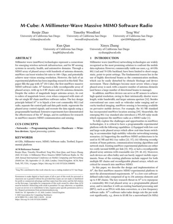
M-Cube: A Millimeter-Wave Massive MIMO Software RadioRenjie ZhaoTimothy WoodfordTeng Wei University of California San Diegor2zhao@ucsd.eduUniversity of California San Diegotwoodfor@ucsd.eduUniversity of California San Diegosjwt2009@gmail.comKun QianXinyu ZhangUniversity of California San Diegokuq002@ucsd.eduUniversity of California San Diegoxyzhang@ucsd.eduABSTRACT1Millimeter-wave (mmWave) technologies represent a cornerstonefor emerging wireless network infrastructure, and for RF sensingsystems in security, health, and automotive domains. Through aMIMO array of phased arrays with hundreds of antenna elements,mmWave can boost wireless bit-rates to 100 Gbps, and potentiallyachieve near-vision sensing resolution. However, the lack of anexperimental platform has been impeding research in this field. Thispaper fills the gap with M 3 (M-Cube), the first mmWave massiveMIMO software radio. M 3 features a fully reconfigurable array ofphased arrays, with up to 8 RF chains and 256 antenna elements.Despite the orders of magnitude larger antenna arrays, its costis orders of magnitude lower, even when compared with state-ofthe-art single RF chain mmWave software radios. The key designprinciple behind M 3 is to hijack a low-cost commodity 802.11adradio, separate the control path and data path inside, regenerate thephased array control signals, and recreate the data signals using aprogrammable baseband. Extensive experiments have demonstratedthe effectiveness of the M 3 design, and its usefulness for researchin mmWave massive MIMO communication and sensing.Millimeter-wave (mmWave) networking technologies are widelyrecognized as the most promising solution to confront the mobiledata explosion. However, commercially viable use cases, e.g., 60 GHz802.11ad and 70 GHz backhaul, have been limited to short-range,static, point-to-point settings. The fundamental reason lies in theuse of highly directional beams as the communication medium,which can be easily disturbed by obstacle blockage and devicemovement. These challenges become most severe when a largephased array is used, with a massive number of antenna elements(and hence a large number of directional beams to manage).In addition, mmWave devices can serve as RF sensors to achievehigh spatial resolution, owing to their intrinsically shorter wavelength, wider bandwidth, and larger antenna aperture [32]. Besidesconventional use cases such as vehicular radar ranging and security/medical imaging, mmWave sensing is becoming availableon pervasive mobile devices. For example, the 5G NR standardhas incorporated mmWave location sensing [59]. Meanwhile, theemerging 802.11ay standard also introduces a WLAN radar modewhich repurposes the mmWave radio as a MIMO radar [1].To fully explore the challenges and opportunities in mmWavetechnologies, it is critical to have a programmable experimentalplatform with the following capabilities: (i) Equipped with low-costand large-scale phased arrays which allow real-time beam switching, to accommodate high mobility vehicular networking/sensingscenarios; (ii) Supporting the mmWave MIMO architectures to beused in 5G NR and 802.11ay radios [22, 37]; (iii) Allowing reconfiguration of beam patterns, communication/sensing algorithms andnetwork stack. Existing mmWave experimental platforms are eithertoo costly (around 200K per link [33, 39]), or lack a reconfigurablephased array antenna with reasonable size [39, 48, 65]. Moreover,such devices are often bulky and can barely support mobile experiments. None of the existing platforms include support for bothmultiple RF chains and reconfigurable phased arrays, which arecritical for research into mmWave MIMO.In this paper, we describe the design and implementation ofM 3 , the first mmWave massive MIMO experimental platform tomeet the aforementioned requirements. M 3 is a low-cost softwaredefined radio/radar comprised of up to 256 antenna elements andup to 8 RF chains. The key research thrust in M 3 is to repurposea commodity 802.11ad phased array as a programmable phasedarray, and to interface it with an existing baseband processing unit(BPU), such as an FPGA with data converters, or a low-frequencysoftware radio. M 3 ’s software radio/radar design cuts the per-nodecost significantly, e.g., down to 3.8K for a narrowband (56 MHz)CCS CONCEPTS Networks Programming interfaces; Hardware Wireless devices; Signal processing systems.KEYWORDS60 GHz, Millimeter-wave, MIMO, Software radio, Testbed, Experimental platformACM Reference Format:Renjie Zhao, Timothy Woodford, Teng Wei, Kun Qian, and Xinyu Zhang.2020. M-Cube: A Millimeter-Wave Massive MIMO Software Radio. In The26th Annual International Conference on Mobile Computing and Networking(MobiCom ’20), September 21–25, 2020, London, United Kingdom. ACM, NewYork, NY, USA, 14 pages. https://doi.org/10.1145/3372224.3380892 TengWei contributed to this work when he was a visiting student in UC San Diego.Permission to make digital or hard copies of all or part of this work for personal orclassroom use is granted without fee provided that copies are not made or distributedfor profit or commercial advantage and that copies bear this notice and the full citationon the first page. Copyrights for components of this work owned by others than ACMmust be honored. Abstracting with credit is permitted. To copy otherwise, or republish,to post on servers or to redistribute to lists, requires prior specific permission and/or afee. Request permissions from permissions@acm.org.MobiCom ’20, September 21–25, 2020, London, United Kingdom 2020 Association for Computing Machinery.ACM ISBN 978-1-4503-7085-1/20/09. . . UCTION
MobiCom ’20, September 21–25, 2020, London, United KingdomRenjie Zhao, Timothy Woodford, Teng Wei, Kun Qian, and Xinyu ZhangControl antenna stateControl SignalBasebandmoduleCoaxialCableTo spectrum analyzerFrom baseband moduleReference clockTo phased array moduleIF data signalCarry baseband signalIperf clientIperf serverBasebandmodulePhased arraymodulePhased arraymoduleFigure 1: Architecture of an 802.11ad mmWave radio.2 RF-chain 72-antenna mmWave MIMO, and below 15K for awideband (4 GHz) 4 RF-chain 128-antenna version.The key observation behind the M 3 design is that many modernmmWave radios [9, 42] adopt a split-IF (intermediate frequency)architecture as shown in Fig. 1. The baseband-to-IF and IF-to-RFplus-antenna modules, henceforth referred to as baseband module(BM) and phased array module (PM), are realized in two separatechips, connected through a single coaxial cable that carries both dataand control signals. By reverse engineering the control channel, andregenerating the control signals using an external FPGA, we gainfull access to the phased array, including reconfiguring its codebookentries (beam patterns), triggering beam scanning, selecting andswitching between the beam patterns in real-time, and tuning theindividual antenna element gain. For the data channel, we replacethe original 802.11ad BM with a customized BPU, along with abridge board that interfaces the BPU and the PM. The bridge boardis designed such that it can take as input/output either baseband I/Qsignals or modulated RF signals below 4 GHz. With this board, thelow-cost commodity phased array can be attached to any existingBPU, such as a USRP, WARP, or customized FPGAs.To extend this architecture to a mmWave MIMO setup, we foundthat recently emerged multi-phased-array 802.11ad radios [3, 30]provide the same data channel to multiple carrier-synchronizedphased arrays, and can switch on one or more of them simultaneously. By interfacing each phased array to a separate bridge boardand separate ADC/DAC channel on the BPU, we can construct a hybrid beamforming architecture with up to 8 RF chains, each attachedto a 6 6 phased array. Furthermore, by clock-sharing between thetransmitter and receiver path, we can convert an M 3 node intoa software-defined mmWave MIMO radar with a massive numberof phased array elements. In addition, the phased arrays can berearranged into a ring or cube layout, to expand the field-of-viewto the entire 3D space.We have conducted comprehensive measurement and testing tovalidate the feasibility and effectiveness of the M 3 design. Our keyfindings include: (i) Reconfigurability. After a one-time calibration,the multiple phased arrays on M 3 can be reconfigured separatelyto generate desired beam widths and directions. M 3 enables realtime mmWave MIMO communication, channel measurement, andradar sensing. (ii) Control path performance. M 3 can control thebeam switching in real-time with a latency of 412 ns, which iscommensurate with commodity 802.11ad radios. (iii) Data pathperformance. The bridge board design in M 3 does not degrade thephase noise and signal to noise ratio (SNR) level. Depending on thesampling frequency of the BPU, it can achieve an end-to-end SNRof 19 dB.Figure 2: Measurement setup to anatomize a commoditysplit-IF 802.11ad radio.Furthermore, we conducted two case studies to demonstrate theapplication of M 3 in exploring mmWave MIMO networking andsensing systems. (i) Context-aware mmWave MIMO hybrid beamforming. We implement a mmWave MIMO OFDM framework tocharacterize the single-user MIMO and multi-user MIMO performance in indoor/outdoor environments. Our experiments revealthe need for multipath context-aware MIMO mode adaptation. (ii)mmWave MIMO radar with uniform and non-uniform array layout.We implement a multi-phased-array radar with non-uniform arraylayout, and demonstrate its higher angular resolution in comparisonwith single array or uniform arrays.The key contributions of M 3 can be summarized as follows: (i)Designing the data path to bridge programmable baseband processors with low-cost commodity phased array modules. (ii) Designingthe control path to reconfigure and control the phased array withsub-µs latency. (iii) Restructuring the commodity 802.11ad radiointo a massive MIMO mmWave radio/radar. (iv) Experimental verification of the M 3 architecture and performance, along with newmeasurement insights for mmWave MIMO radio/radar systems. Toour knowledge, M 3 represents the first-of-its-kind programmablemmWave MIMO platform. We will follow the WARP project model[54] to make M 3 available to the wireless research community,through open-source hardware and paid fabrication/assembly services. The code, documentation and further information will bereleased through the project website, http://m3.ucsd.edu/sdr/.2ANATOMY OF COMMODITY 802.11ADMMWAVE RADIOThis section presents our reverse engineering work on a commodity802.11ad radio, which serves as the basis of the M 3 design.Mainstream 802.11ad network interface cards (NICs) [9, 38, 58]all follow a modular split-IF architecture as illustrated in Fig. 1.The NIC comprises two modules connected via a coaxial cable: abaseband module (BM), which converts between baseband signalsand IF signals; and a phased array module (PM), comprised of thephased array antenna and RF front-end (converting between the IFsignals and 60 GHz RF signals). Unlike low-frequency radios, theantenna and RF chain are integrated on the same module ratherthan connected via a cable because routing mmWave signals acrosseven a few millimeters leads to high losses [42].To tap into the PM, we use a spectrum analyzer (Keysight E4448A)to monitor the coaxial interface on a commodity 802.11ad radio fromAirfide Inc. [3], which realizes the split-IF architecture through adual-chip solution—A Qualcomm QCA6335 baseband, and QCA6310RF front-end integrated with one or more 6 6 phased arrays. As
M-Cube: A Millimeter-Wave Massive MIMO Software RadioMobiCom ’20, September 21–25, 2020, London, United KingdomIF Bridge BoardDCBasebandmoduleControl Signal@ 118MHzHarmonicsReference ClockIF Data Signal f@ 7.5GHz@ 15GHzFigure 3: Spectrum content of the coaxial cable between thebaseband module and phased-array front-end on a commodity 802.11ad xerIF GeneratorX6TriplexerMACPHYPhased Array ModuleAmplifiersBeamformerBaseband ModuleControlRadioFigure 4: Schematic of the Tx RF chain on the commodity802.11ad radio (Rx chain is similar).shown in Fig. 2, we use a 3-port splitter (Pomona #72969), SMAadapters and cables to enable the spectrum analyzer to “eavesdrop”on the coaxial cable between the BM and PM. The radio transmitsdata continuously through iPerf, while the normal 802.11ad protocols are in operation (e.g., beam scanning). The spectrum content(Fig. 3) shows that the coaxial cable carries 4 types of signals: aDC power supply, an IF reference clock at around 7.5 GHz, control signals around 118 MHz, and IF data signals around 15 GHz.The spectrum composition shares similar principles with a recentsplit-IF 802.11ad chipset design from Broadcom [9], although withdifferent frequency planning and phased array structure. Basedon our measurement and insights from [9], the schematic of theQualcomm 802.11ad NIC can be reconstructed as in Fig. 4. Belowwe present an anatomy of the signals passing between the BM andPM.Control signal: This signal configures key parameters of thePM, customizing the codebook, beam selection, RF gain, poweramplifier gain on individual antennas, probing the phased arraystatus, etc. The NIC is usually attached to a host PC through PCIeM.2. Parameter configuration is initiated by issuing a wireless module interface (WMI) command [44] from the host PC running thewil6210 802.11ad driver [25]. The firmware on the BM receives thecommand and forwards it to the PM. Both hardware modules havea digital modem for control commands, which manages the modulation/demodulation, error correction, etc. The modulated controlsignal resides on a low frequency (118 Msps symbol rate) to avoidinterference with the data channel. The control channel allows fortwo modes of operation: (i) Register read-write mode, wherein theBM can control/probe the status of the PM; (ii) Streaming mode,wherein a customized codebook matrix can be loaded from the BMto the PM. The PM maintains a simple state-machine that sets thestatus of the digital modem.IF data signal: As in typical superheterodyne radios, the commodity 802.11ad transmitter first converts the baseband I/Q signalHost PC90 X2Phased ArrayBPUSync Control ModuleFPGAFigure 5: Schematic of a single Tx RF chain on the M 3mmWave MIMO software-radio (Rx chain is similar).to an IF analog I/Q signal, at IF carrier frequency 15 GHz (2 thereference clock signal passing through the coaxial interface). Therefore, we can send arbitrary signals through the PM, as long as theyare within the passband centered at 15 GHz. The PM integratesIF-to-RF up/downconversion chains, IF amplifiers, power management units, as well as the necessary building blocks for the phasedarray itself (e.g., phase shifters and RF power amplifiers).Reference clock: Mainstream mmWave chipsets [9, 13, 14] typically use a sliding IF architecture to achieve mmWave signal upconversion and channelization. In the Qualcomm 802.11ad radio,the BM provides a reference clock around 7.5 GHz (switching between 7.29, 7.56, 7.83 and 8.10 GHz) to the PM, enabling it to switchamong the four 802.11ad channels (centered at carrier frequencies 58.32, 60.48, 62.64 and 64.80 GHz). The reference clock signalpasses through the coaxial cable, and then a 6 multiplier is usedto generate the local oscillator (LO) for the PM. For example, with7.56 6 45.36 GHz LO and 7.56 2 15.12 GHz IF signal, theoutput RF signal is 45.36 15.12 60.48 GHz.3OVERVIEW: M 3 ARCHITECTUREIn order to transform the commodity 802.11ad radio into a softwareradio, our basic idea is to reuse the baseband module as a clock/powergenerator and boot loader, but regenerate the control signal using anFPGA-based digital controller, and create a customized data channel by using a programmable BPU plus a baseband-to-IF converter(referred to as a bridge board).As a fundamental architectural level design choice, M 3 separates the data channel and control channel and makes both reconfigurable. As illustrated in Fig. 5, the Tx bridge board reuses the802.11ad BM’s 7.5 GHz clock signal as a clock source, and convertsit to 15 GHz IF. It then takes the BPU’s baseband I/Q signal or modulated low-frequency signal as input, and mixes it with the IF clocksignal to create data signal at 15 GHz IF. As for the control path,we reverse engineer the control channel waveform, and regeneratethe control commands using a low-profile control FPGA. The bridgeboard then combines all three signal paths–the 15 GHz IF datasignal, the 118 MHz control signal, and the 7.5 GHz clock and 3.3 VDC power supply from the BM, and injects them into the PM. TheRx path follows the same architecture with a reversed data pathdirection.This single RF-chain design can be easily extended to a multi-RFchain MIMO mmWave architecture as illustrated in Fig. 6. In MIMOmode, the same 7.5 GHz clock source and power source is generatedby a single QCA6335 802.11ad BM and shared among multiple PMs,ensuring carrier synchronization at RF frequencies. Each RF-chain
MobiCom ’20, September 21–25, 2020, London, United KingdomRenjie Zhao, Timothy Woodford, Teng Wei, Kun Qian, and Xinyu ZhangIF Bridge Board Phased Array ModuleBasebandmoduleControlFPGABPUFigure 6: Integrating multiple RF chains to form the MIMOmmWave RF front-end.has a separate control channel and data channel, generated by thecontrol FPGA and a multi-channel BPU, respectively. A similar architecture can be used to build a software-defined mmWave MIMOradar.In terms of cost, we note that the commodity Airfide 802.11adradio (comprised of 8 phased arrays, 256 antenna elements in total) costs below 700 [3]. Four pairs of Tx and Rx bridge boardprototypes cost around 1.8K for the components, 650 for PCB fabrication and 1.3K for assembly (price drops significantly as volumeincreases). So the necessary RF front-end building blocks to realize4 4 mmWave MIMO (256 elements) only costs 4.5K in total. Alower profile 2 2 MIMO and single RF chain cost 2.6K and 1.6K,respectively. When counting the BPU cost, a narrow bandwidth2 2 MIMO (e.g., using USRP B210, a 2-channel 56 MHz BPU at 1.2K) costs only 3.8K. Even when counting the high-profile 4channel BPU USRP N310 ( 10K, 125 MHz bandwidth) or 4-channelXilinx UltraScale RFSoC ( 9K, 4 GHz bandwidth), the entire 4 4mmWave MIMO software radio (with 256 Tx/Rx antenna elements)costs below 15K. The cost is significantly lower even when compared with the state-of-the-art single RF-chain platforms such asX60 [39] ( 170K, 12-element phased array), and OpenMili ( 15K,4-element phased array) [65, 66].4DATA PATH DESIGNIn this section, we describe the data path design in detail. Withoutloss of generality, our description focuses on the Tx path. The Rxpath simply follows the reverse flow.4.1Bridge Board DesignAs shown in Fig. 7, the bridge board comprises three paths. Path 1connects the QCA6335 BM directly to the QCA6310 PM. Throughthis path, the BM provides the 3.3 V DC power supply, and 7.5 GHzreference clock for the carrier LO generation at the PM. The normalcontrol commands, such as loading a customized codebook, canstill be issued from a PC host, routed by the BM through this path,and eventually executed by the PM.Path 2 is the bridging path, which uses the 7.5 GHz referencesignal from the BM to generate the IF data signal. The referenceclock is generated from the on-chip PLL of QCA6335, optimized forhigh stability and low phase noise. By avoiding regenerating theclock, we can reduce the complexity and cost of the bridge boardsubstantially. To generate the IF data signal, the reference clocksignal first goes through a 2 frequency multiplier to generate theControlFPGABasebandmodulePath 3Path 1-2dBBPFPhased arraymoduleOff BoardOn BoardPath 220dB20dBHPFX2MixerFigure 7: High level schematic of the bridge board and offboard connection.15 GHz IF clock, which is then mixed with baseband data signalsthrough a passive image rejection I/Q mixer HMC8191.Before the mixer, a 6850-7850 MHz band pass filter (BPF) BFCN7331 is chosen to reject the signals other than the reference clock.However, BFCN-7331 has a return loss of 0.13 dB @100 MHz(around 97.3% power reflected) [31], which will cause strong reflections to the 118 MHz control signals, creating an interfering “multipath” effect. Therefore, a 2 dB 0-25 GHz attenuator HMC652LP2Eis placed before the BPF to weaken the reflected signal to preventit from corrupting the control commands.We chose the passive I/Q mixer HMC8191, because it interoperates with a wide range of LOs (6 GHz to 26.5 GHz) and canbe used for direct I/Q modulation or image reject mixing, neededby the homodyne and heterodyne interfaces to the BPU (Sec. 4.2).The mixer requires a stable 14-20 dBm LO to achieve stable performance, so we use an active 2 frequency multiplier HMC814which has flat 17 dBm output over 2-6 dBm input. Consideringthe around -30 dBm reference clock input, 2 dB attenuation and1.5 dB insertion loss of the BPF, two additional 20 dB amplifiersPMA3-83LN are used to reach 30 2 1.5 20 20 6.5 dBmpower, which matches the input requirement of the 2 multiplier.Besides the 15 GHz signal, the output of the mixer also contains asignal at the 7.5 GHz fundamental frequency, which acts as a noiseto the reference clock to the phased array module. We thus add a13-19 GHz wideband high pass filter (HPF) XHF-143M at the output of this path to filter out this noise. This is a reflectionless filterwith around 26 dB return loss at 100 MHz (0.2% power reflection).The reflection of HPF is much lower than BFCN-7331 and will notdestroy the control signal.Path 3 routes control commands from the control FPGA tothe PM. Although the BM can send control commands throughpath 1, path 3 is still necessary for real-time control, as detailed inSec. 5. In current version of the bridge board, path 1 and path 3 areimplemented with off-board coaxial components to preserve theflexibility of signal strength balancing. These components will beintegrated to a PCB in a future version, making the bridge boardeven more compact.In the prototype version, we utilize off-board connectors for moreconvenient debugging and circuit performance evaluation (Fig. 7).Path 1 and 3 pass through the off board connection and the splittersare using Tee connectors which has low isolation. Although a powersplitter with higher isolation would solve the reflected signal issueintroduced in path 2, the available ultra wideband splitter coveringall the signals locating from DC up to 15 GHz would introduce
M-Cube: A Millimeter-Wave Massive MIMO Software Radio(a)IF Bridge Board(b)IF Bridge Board90 X2QADC/ ADC/DAC DACADC/ ADC/DAC DACIIF1Sub-6GHzRF front-endIF2BPUFigure 8: Bridging path architecture: (a) homodyne and (b)heterodyne.additional insertion loss. Then the reference clock and basebandcommand power would be too low for the RF module to receivethem.The Rx bridge board shares most of its components with thereverse signal path, except that two 5-18 GHz 13 dB amplifiers (AVA183A ) are added between the HPF and mixer to ensure properinput power to the BPU.4.2TXIF band CFODesired90 X2BPUMobiCom ’20, September 21–25, 2020, London, United KingdomBridging Path ArchitectureThe single bridge board design mentioned above can fit into twodifferent architectures along path 2: homodyne and heterodyne,interfacing with BPUs that generate dual-channel I/Q signals andsingle-channel low IF signals, respectively.4.2.1 Homodyne Architecture. In the homodyne architecture (Fig. 8(a)),the baseband I/Q signals are directly upconverted to IF with a quadrature LO, which is generated by the mixer using the 15 GHz reference. This architecture is widely used by modern sub-6 GHz radiosbecause it is simple, has lower cost and no image problem.We chose the HMC8191 mixer with DC to 5 GHz IF bandwidth,to ensure interoperability with the wideband I/Q input from DACcentered at DC. The upconverted double side band signal centeredat 15 GHz will also be able to pass through the HPF. Note that thefilter chosen here is for a wideband use case. An additional lowpass filter will be needed at baseband to filter out the harmonicscaused by the discrete signal generated by DAC.We implement this homodyne architecture using two differentBPUs built by combining an ADC/DAC module with an FPGA. (i)The FMC150 BPU uses a Virtex-6 LX240T FPGA with an FMC150ADC/DAC board supporting a 40 Msps I/Q sampling rate. We developed the FPGA bitstream to be compatible with the WARP v3[28] PC host driver. (ii) The FMCDAQ2 BPU uses a Xilinx KCU105development board with an FMCDAQ2 1 Gsps ADC/DAC a KintexUltrascale XCKU040 FPGA running the open-source FPGA bitstream developed in [65]. Detailed evaluation of M 3 with theseBPUs is in Sec. 9. It is possible to achieve a sampling rate compatible with 802.11ad or 802.11ay, e.g. using Xilinx Zynq UltraScale RFSoC [62] which has 8 4 Gsps ADCs and 8 6.5 Gsps DACs, butthis is beyond the scope of our current work.4.2.2 Heterodyne Architecture. For the heterodyne architecture, alow-frequency software-defined radio (SDR), e.g., USRP, first generates a carrier-modulated first-stage sub-6 GHz IF signal, then thebridge board acts as a second stage IF mixer to upconvert the signalinto the desired 15 GHz IF data signal.Unfortunately, we cannot directly interface the single-outputsignal from the SDR with the dual-input quadrature mixer on theRXImageCFO CFOfffT f RFigure 9: In the heterodyne architecture, upconversion atthe Tx bridge board produces two components in IF band.Due to CFO, downconversion at the Rx board imperfectlycombines the two components, which severely reduces SNR.bridge board as shown in Fig. 8(b) due to an image problem. As illustrated in Fig. 9, consider a Tx SDR generating a signal m(t)sin(2π f t),with first stage IF f and baseband signal m(t). With Tx LO fT , thesignal at IF band is:m(t)sin(2π f t)sin(2π fT t) m(t)[cos(2π (fT f )t) cos(2π (fT f )t)],2which has two components at frequency fT f and fT f calleddesired signal and image signal, respectively. When f 2 GHz,the two components are both located in the passband of the filterson bridge board and the phased array (i.e., 13 GHz 17 GHz), soboth components will be transmitted through the phased array.This image incurs two problems: (i) it will cause a waste on thefrequency band. (ii) it will introduce “self-interference” at the RXside when carrier frequency offset (CFO) exists. More specifically,at the Rx side, the signal is downconverted from IF using carrierfrequency f R to become:m(t)[cos(2π (fT f )t) cos(2π (fT f )t)]sin(2π f R t) 2m(t)[sin(2π (f (f R fT ))t) sin(2π (f (f R fT ))t)].4Because there is no way to perfectly eliminate the CFO, the desired and image signal components are separated by 2 (f R fT ).Since the CFO value (f R fT ) is typically tens of kHz, the two components will be offset in frequency domain and thus interfere witheach other where they overlap. There is no simple post-processingsolution to separate them, so the final SNR will be extremely low.In M 3 , we explore two methods to overcome this challenge onthe Tx side:(i) Adding a 90 hybrid coupler between the bridge board andthe baseband SDR to leverage the image rejection function of theHMC8191 mixer. The 90 hybrid coupler divides the single-channellow-IF signal into two channels with a 90 phase offset, which arethen fed into IF1 and IF2 respectively as in Fig. 8(b). The outputsignal from the bridge board becomes:m(t)m(t)sin(2π f t)sin(2π fT t) cos(2π f t)cos(2π fT t) 22m(t)cos(2π (fT f )t).2which is the desired single side band signal.(ii) Taking advantage of a built-in filter to reject the image signal.By sweeping a wide frequency range using a high-frequency signalgenerator, we found the QCA6310 PM contains a bandpass filterwith a passband of 12 17 GHz. Therefore, if the LO frequency is15.12 GHz, the image signals will be directly filtered if the BPU
-20Original-40-20-40-60(a)Strength (dBm)Strength (dBm)MobiCom ’20, September 21–25, 2020, London, United KingdomRenjie Zhao, Timothy Woodford, Teng Wei, Kun Qian, and Xinyu ZhangWith 000000001111000101111101111025dB35dB-6012 14 16 18Frequency (GHz)(b)12 14 16 18Frequency (GHz)Figure 10: Image rejection of original, higher IF filtered (35dB) and using 90 hybrid (25 dB).output is above 17 15.12 1.88 GHz. This can be easily satisfiedon popular BPUs such as USRP and WARP (output up to 5.8 GHz).To verify the effectiveness of these two methods, we connecta Tx PM (15.12 GHz IF) to a bridge board, and then use a signalgenerator to generate the low-IF in three setups: (i) 1 GHz singletone to one port of the bridge board, (ii) 1 GHz single tone to twoports of the bridge board through a 90 hybrid coupler (KRYTAR3005040), (iii) 2.4 GHz single tone to one port of the bridge board.Meanwhile, we connect an Rx PM like the “eavesdrop” setup introduced in Sec. 2 , and plot the result in Fig. 10. Fig. 10(a) showsthe double side band received signal at 1 GHz. The image signalhas comparable strength with the desired signal. Fig. 10(b) showsthe effectiveness of two methods: adding a hybrid coupler leads toaround 25 dB image rejection, which is aligned with the HMC8191performance specification [6]. Using a 2.4 GHz first-stage IF willhave around 35 dB image rejection, which will not impede normaldata transmissions since the end-to-end SNR is usually much lower.We expect the performance can be further enhanced by combiningthe two aforementioned methods.Since adding an additional hybrid coupler or filter will introducemore insertion loss, we need to consider this in the gain budgetcalculation. For the TX bridge board, the circuit will introducemixer conversion loss (10 dB), BPF loss (2 dB), and splitting loss(4 dB). To reach the same 15 GHz IF signal strength (
(MobiCom '20), September 21-25, 2020, London, United Kingdom. ACM, New . for profit or commercial advantage and that copies bear this notice and the full citation . M-Cube: A Millimeter-Wave Massive MIMO Software Radio MobiCom '20, September 21-25, 2020, London, United Kingdom .