Transcription
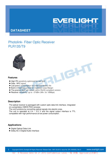
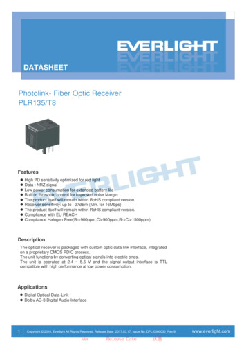
Photolink- Fiber Optic ReceiverPLR135/T9Features High PD sensitivity optimized for red lightData : NRZ signalLow power consumption for extended battery lifeBuilt-in threshold control for improved noise MarginThe product itself will remain within RoHS compliant version.Receiver sensitivity: up to –27dBm (Min. for 16Mbps)DescriptionThe optical receiver is packaged with custom optic data link interface, integratedon a proprietary CMOS PDIC process.The unit functions by converting optical signals into electric ones.The unit is operated at 2.4 5.5 V and the signal output interface is TTLcompatible with high performance at low power consumption.Applications Digital Optical Data-Link Dolby AC-3 Digital Audio Interface1Copyright 2010, Everlight All Rights Reserved. Release Date : MAY.30.2013. Issue No: DPL-0000025 Rev.8www.everlight.com
DATASHEETPhotolink- Fiber Optic ReceiverPLR135/T9Absolute Maximum Ratings (Ta 25 )ParameterSymbolRatingUnitSupply VoltageVcc-0.5 5.5VOutput VoltageVoutVcc 0.3VStorage TemperatureTstg-40 to 85ºCOperating TemperatureTopr-20 to 70ºCSoldering TemperatureTsol260*ºCHuman Body Model ESDHBM2000VMachine Model ESDMM100VNotes: Soldering time 10 seconds.Recommended Operating ConditionsParameterSupply .50VElectro-Optical Characteristics (Ta 25 ,Vcc 3V, CL 5pf)ParameterSymbolConditionsMIN.TYP.MAX.UnitPeak sensitivity wavelength p--650-nmTransmission Distanced*10.2--5mMaximum receiver powerPc,maxRefer to Fig.1---14dBmMinimum receiver powerPc,minRefer to Fig.1-27--dBmIccRefer to Fig.2-412mAHigh level output voltageVOHRefer to Fig.32.12.5-VLow level output voltageVOLRefer to Fig.3-0.20.4VRise timetrRefer to Fig.3-1020nsFall timetfRefer to Fig.3-1020nsPropagation delay Low to HightPLHRefer to Fig.3--120nsPropagation delay High to LowtPHLRefer to Fig.3--120nsPulse Width Distortion twRefer to Fig.3-25- 25ns tjRefer to Fig.3, Pc -14dBm-115nsJitterRefer to Fig.3, Pc -27dBm-520nsNRZ signal0.1-16Mb/sDissipation currentTransfer rate2TCopyright 2010, Everlight All Rights Reserved. Release Date : MAY.30.2013. Issue No: DPL-0000025 Rev.8www.everlight.com
DATASHEETPhotolink- Fiber Optic ReceiverPLR135/T9Measuring Method*Fig.1 Measuring Method of Maximum and Minimum Input Power that Receiver Unit NeedControl CircuitStandard plastic optic fiber cableTransmitterPLR135 Receiver UnitOptical Power Meter*Fig.2 Measuring Method of Dissipation CurrentStandard plastic optic fiber cableStandard Transmitter UnitVinVccPLR135 Receiver UnitGNDVccA16 Mbps NRZ "0101" successive signal input3Vout0.1uF47uHSignalInputGND3VCopyright 2010, Everlight All Rights Reserved. Release Date : MAY.30.2013. Issue No: DPL-0000025 Rev.8www.everlight.com
DATASHEETPhotolink- Fiber Optic ReceiverPLR135/T9*Fig.3 Measuring Method of Output Voltage, Pulse and JitterStandard plastic optic fiber cableStandard Transmitter UnitVinVccPLR135 Receiver UnitGNDVccVout0.1uF47uHSignalInputGNDA3V16 Mbps NRZ "0101" successive signal inputTPHLTPLHInputCH150%CH2Output50%tj1tj2tw TPHL-TPLHApplication Circuit(1) General application circuit for Vcc 3V (2) General application circuit for Vcc 5VReceiver UnitReceiver outC1:0.1uFC2:30pF (Suggestion)L2:47uHNote: For having good coupling, the C1,C2 capacitor must be placed within 7mm4Copyright 2010, Everlight All Rights Reserved. Release Date : MAY.30.2013. Issue No: DPL-0000025 Rev.8www.everlight.com
DATASHEETPhotolink- Fiber Optic ReceiverPLR135/T9Typical Electro-Optical Characteristics Curves*Fig.4 Power supply voltage vs. Minimumreceiver powerOptical Input Sensitivity (dBm)Operating Voltage Vcc 3.3V-28-26-24-22-202.0Transfer rate vs. Minimum receiverpower-32Operating Transfer Rate16Mbps25Mbps-30Optical Input Sensitivity rating Voltage (V)5.05.56.00510152025Transfer Rate (Mbps)Note: Before using the PLR135 device, please confirm the minimum sensitivity at different operating voltageand transmission rate.5Copyright 2010, Everlight All Rights Reserved. Release Date : MAY.30.2013. Issue No: DPL-0000025 Rev.8www.everlight.com
DATASHEETPhotolink- Fiber Optic ReceiverPLR135/T9Package DimensionNotes: 1. All dimensions are in millimeters.2. General Tolerance : 0.3mmPCB Layout for Electrical CircuitNotice:1. Unit:mm2. PCB tolerance:1.6mm6Copyright 2010, Everlight All Rights Reserved. Release Date : MAY.30.2013. Issue No: DPL-0000025 Rev.8www.everlight.com
DATASHEETPhotolink- Fiber Optic ReceiverPLR135/T9Label Explanation‧CPN: Customer’s Product NumberPb‧P/N: Product NumberEVERLIGHTXCPN :P N:RoHSPLR135/T9QTY :CAT :HUE :REF :LOT NO :‧QTY: Packing Quantity‧CAT: Luminous Intensity Rank‧HUE: Dom. Wavelength Rank‧REF: Forward Voltage Rank‧LOT No: Lot Number‧X: MonthReference :‧Reference: Identify Label NumberPacking Quantity Specification1. 50 pcs/tube2. 20 tubes/box3. 4 boxes/cartonNotes1. Above specification may be changed without notice. EVERLIGHT will reserve authority on material change for abovespecification.2. When using this product, please observe the absolute maximum ratings and the instructions for using outlined in thesespecification sheets. EVERLIGHT assumes no responsibility for any damage resulting from use of the product whichdoes not comply with the absolute maximum ratings and the instructions included in these specification sheets.3. These specification sheets include materials protected under copyright of EVERLIGHT corporation. Please don’treproduce or cause anyone to reproduce them without EVERLIGHT’s consent.7Copyright 2010, Everlight All Rights Reserved. Release Date : MAY.30.2013. Issue No: DPL-0000025 Rev.8www.everlight.com
DATASHEETPhotolink- Fiber Optic ReceiverPLR135/T9Application Notes: PLR135 Series PCB layout for motherboard integrationTo achieve better jitter and low input optical power performances, several PCB layout guidelines must be followed.These guidelines ensure the most reliable PLR135 POF performance for the motherboard integration. Failed to implementthese PCB guidelines may affect the PLR135 jitter and low input power performances.1.Careful decoupling of the power supplies is very important. Place a 0.1uf surface mount (size 805 or smaller)capacitor as close as (less than 2cm) to the POF Vdd and Gnd leads. The 0.1uf act as a low impedance path toground for any stray high frequency transient noises.2.To reduce the digital noises form the digital IC on the motherboard, the planar capacitance formed by an isolated Vccand Gnd planes is critical. The POF device must be mounted directly on these two planes to reduce the lead parasiticinductance.3.The isolated Vdd and Gnd planes must be connected to the main Vcc and Gnd (digital) planes at a single point usingferrite beads. The beads are used to block the high frequency noises from the digital planes while still allowing the DCconnections between the planesEVERLIGHT ELECTRONICS CO., LTD.Office: No 6-8,Zhonghua Rd., Shulin Dist.,New Taipei City 23860, Taiwan, R.O.C8Tel: 886-2-2685-6688Fax: 886-2-2685-6897http://www.everlight.comCopyright 2010, Everlight All Rights Reserved. Release Date : MAY.30.2013. Issue No: DPL-0000025 Rev.8www.everlight.com
Standard Transmitter Unit Input Signal Input t w T PHL-T PLH tj1 tj2 50% 50% CH2 47uH T PLH T PHL Vcc GND CH1 Standard plastic optic fiber cable PLR135 Receiver Unit 3V A GND 0.1uF Vcc Vout Application Circuit (1) General application circuit for Vcc 3V (2) General application circuit for Vcc 5V L2:47uH C1:0.1uF Vout 3V L2 Vcc GND C1 Receiver Unit
![Fiber Optic - Perimeter Intrusion Detection System [Fopids]](/img/57/foss-presentation.jpg)