Transcription
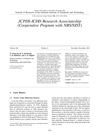
Volume 106, Number 6, November–December 2001Journal of Research of the National Institute of Standards and Technology[J. Res. Natl. Inst. Stand. Technol. 106, 997–1012 (2001)]Electron DiffractionUsing Transmission Electron MicroscopyVolume 106Leonid A. Bendersky and FrankW. GayleNational Institute of Standards andTechnology,Gaithersburg, MD t.gov1.Number 6November–December 2001Electron diffraction via the transmissionelectron microscope is a powerfulmethod for characterizing the structure ofmaterials, including perfect crystals anddefect structures. The advantages of electron diffraction over other methods, e.g.,x-ray or neutron, arise from the extremelyshort wavelength (艐2 pm), the strongatomic scattering, and the ability to examine tiny volumes of matter (艐10 nm3).The NIST Materials Science and Engineering Laboratory has a history of discoveryand characterization of new structuresthrough electron diffraction, alone or incombination with other diffraction methods.This paper provides a survey of some ofthis work enabled through electron microscopy.Key words: crystal structure; crystallography; defects; electron diffraction; phasetransitions; quasicrystals; transmissionelectron microscopy.Accepted: August 22, 2001Available online: http://www.nist.gov/jresIntroductionatomic potential form diffraction spots on the back focalplane after being focused with the objective lens. Thediffracted waves are recombined to form an image onthe image plane. The use of electromagnetic lenses allows diffracted electrons to be focused into a regulararrangement of diffraction spots that are projected andrecorded as the electron diffraction pattern. If the transmitted and the diffracted beams interfere on the imageplane, a magnified image of the sample can be observed.The space where the diffraction pattern forms is calledreciprocal space, while the space at the image plane orat a specimen is called real space. The transformationfrom the real space to the reciprocal space is mathematically given by the Fourier transform.A great advantage of the transmission electron microscope is in the capability to observe, by adjusting theelectron lenses, both electron microscope images (information in real space) and diffraction patterns (information in reciprocal space) for the same region. Byinserting a selected area aperture and using the parallelThe use of electron diffraction to solve crystallographic problems was pioneered in the Soviet Union byB. K. Vainshtein and his colleagues as early as the 1940s[1]. In the elektronograf, magnetic lenses were used tofocus 50 keV to 100 keV electrons to obtain diffractionwith scattering angles up to 3 to 5 and numerousstructures of organic and inorganic substances weresolved. The elektronograf is very similar to a moderntransmission electron microscope (TEM), in which thescattered transmitted beams can be also recombined toform an image. As the result of numerous advances inoptics and microscope design, modern TEMs are capable of a resolution of 1.65 Å for 300 kV (and below 1 Åfor 1000 kV) electron energy-loss combined with chemical analysis (through x-ray energy and electron-lossenergy spectroscopy) and a bright coherent field emission source of electrons.The main principles of electron microscopy can beunderstood by use of optical ray diagrams [2,3], asshown in Fig. 1. Diffracted waves scattered by the997
Volume 106, Number 6, November–December 2001Journal of Research of the National Institute of Standards and TechnologyFig. 1. Optical ray diagram with an optical objective lens showing theprinciple of the imaging process in a transmission electron microscope.Fig. 2. Three observation modes in electron microscope using anobjective aperture. The center of the objective aperture is on theoptical axis. (a) Bright-field method; (b) dark-field method; (c) highresolution electron microscopy (axial illumination).incident beam illumination, we get a diffraction patternfrom a specific area as small as 100 nm in diameter. Therecently developed microdiffraction methods, where incident electrons are converged on a specimen, can nowbe used to get a diffraction pattern from an area only afew nm in diameter. Convergent beam electron diffraction (CBED) uses a conical beam ( 10 3 rad) to produce diffraction disks, and the intensity distribution inside the disks allows unique determination of all thepoint groups and most space groups [4]. Because a selected area diffraction pattern can be recorded fromalmost every grain in a polycrystalline material, reciprocal lattices ( crystal structures) and mutual crystal orientation relationships can be easily obtained. Thereforesingle crystal structural information can be obtained formany materials for which single crystals of the sizessuitable for x-ray or neutron diffraction are unavailable.Such materials include metastable or unstable phases,products of low temperature phase transitions, fine precipitates, nanosize particles etc.In order to investigate an electron microscope image,first the electron diffraction pattern is obtained. Then bypassing the transmitted beam or one of the diffractedbeams through a small objective aperture (positioned inthe back focal plane) and changing lenses to the imagingmode, we can observe the image with enhanced contrast. When only the transmitted beam is used, the observation mode is called the bright-field method (accordingly a bright-field image), Fig. 2a. When onediffracted beam is selected (Fig. 2b), it is called the darkfield method (and a dark field image). The contrast inthese images is attributed to the change of the amplitudeof either the transmitted beam or diffracted beam due toabsorption and dynamic scattering in the specimens.Thus the image contrast is called the absorption-diffraction, or the amplitude contrast. Amplitude-contrast images are suitable to study mesoscopic microstructures,e.g., precipitates, lattice defects, interfaces, and domains. Both kinematic and dynamic scattering theoriesare developed to identify crystallographic details ofthese heterogeneities [2,3].It is also possible to form electron microscope imagesby selecting more than two beams on the back focalplane using a large objective aperture, as shown in Fig.2c. This observation mode is called high-resolution electron microscopy (HREM). The image results from themultiple beam interference (because of the differencesof phase of the transmitted and diffracted beams) and iscalled the phase contrast image. For a very thin specimen and aberration-compensating condition of a microscope, the phase contrast corresponds closely to theprojected potential of a structure. For a thicker specimenand less favorable conditions the phase contrast has to becompared with calculated images. Theory of dynamicscattering and phase contrast formation is now well developed for multislice and Bloch waves methods [5].HREM can be used to determine an approximate structural model, with further refinement of the model usingmuch higher resolution powder x-ray or neutron diffraction. However, the most powerful use of HREM is indetermining disordered or defect structures. Many ofthe disordered structures are impossible either to detector determine by other methods.Other major advantages in using electron scatteringfor crystallographic studies is that the scattering crosssection of matter for electrons is 103 to 104 larger thanfor x rays and neutrons, typical wavelengths (艐2 pm)are one hundredth of those for x rays and neutrons, andthe electron beam can be focused to extremely fineprobe sizes (艐1 nm) [2]. These characteristics meanthat much smaller objects can be studied as single crystals with electrons than with other radiation sources. Italso means a great sensitivity to small deviations froman average structure caused by ordering, structural distortions, short-range ordering, or presence of defects.Such changes often contribute either very weak superstructure reflections, or diffuse intensity, both of whichare very difficult to detect by x-ray or neutron diffraction.998
Volume 106, Number 6, November–December 2001Journal of Research of the National Institute of Standards and TechnologyIn addition, modern transmission electron microscopes provide a number of complementary capabilitiesknown as analytical electron microscopy [6]. Differentdetectors analyze inelasticly scattered electrons (Electron Energy-Loss Spectroscopy, or EELS), excited electromagnetic waves (Energy Dispersion Spectroscopy, orEDS) and Z-contrast that provide information on chemical compositions and local atomic environments. Suchinformation, when combined with elastic electron diffraction, is important in determining structural models,especially when a material consists of multiple phases.In the following sections, various contributions ofNBS/NIST researchers in the field of materials researchwith TEM as a central part of investigation are presented. The emphasis is on crystallographic aspects ofthe research. The presented contributions come mainlyfrom the Materials Science and Engineering Laboratory.2.The discovery of the icosahedral phase triggered aperiod of very active research in the new field of quasicrystals. Many NIST researchers contributed activelyin the early stages, and TEM played an important role inmany aspects of this activity. Shortly after the Shechtman et al. publication, L. Bendersky discovered a different type of quasiperiodic structure—the decagonalphase with a 10-fold rotation axis, which has an apparent 10/mmm point group (Fig. 3) [8]. Electron diffraction analysis of this Al80Mn20 rapidly quenched alloyshowed that the decagonal phase has a structure of twodimensionally quasiperiodic layers, which are stackedperiodically along the ten-fold axis, with a latticeparameter c 1.24 nm. Shortly thereafter, a similardecagonal phase but with a different periodicity(c 1.65 nm) was found in the Al-Pd system [8]. Theimportance of the discovery was not only discovery of anovel structure, but also demonstration of the generalprinciples of quasiperiodicity. Since the discovery of thefirst quasiperiodic structures in Al-Mn alloys in 1984,enormous progress, both experimental and theoretical,has been made. Quasicrystalline phases have been foundin more than hundred different metallic systems, andseveral quasicrystalline phases have been shown to bethermodynamically more stable than periodic crystals[9].Among other significant discoveries at NIST associated with the new field of “quasi-crystallography” were: The first conclusive determination of the m 35 pointgroup for the icosahedral phase (for Al-38 %Mn5 %Si (mass fraction) rapidly solidified alloy) [10].Here the methods of convergent beam electron diffraction (CBED) were applied for the first time to aquasiperiodic structure. Fig. 4 shows an example ofsuch CBED patterns from which the whole (3-dimensional) pattern symmetries of fivefold [1 0], threefold[111] and twofold [001] orientations were derived ( irrational “golden mean” number). Polycrystalline aggregates of a cubic phase [ Al9(Mn,Fe)2Si2] with an overall icosahedral symmetry were found in rapidly solidified Al75Mn15 x Fex Si10(x 5 and 10) alloys [11]. Through a twinning operation, the cubic axes undergo five-fold rotation aboutirrational 1, ,0 axes; however only five orientationsoccur among hundreds of crystals (Fig. 5). This is aspecial orientation relationship without any coincidence (or twin) lattice, and it is dictated by the noncrystallographic symmetry of a motif (in the case ofthe phase—the 54-atom Mackay-icosahedron motif). The motifs are parallel throughout the entire polycrystalline aggregate, and the crystal axes changeacross grain boundaries. Based on this finding, theentire concept of twinning and special grainboundaries was re-examined. A new definition ofDiscovery of New Structures UsingSelected Area and Convergent BeamElectron DiffractionStarting in the early 1980s the Metallurgy Division ofNBS was actively involved in studying the fundamentalsof rapid solidification of a melt. In this process, materials (mostly metallic alloys) crystallize under very rapidcooling conditions (over 104 C/s). Such extreme conditions very often result in the formation of either newmetastable or non-equilibrium crystalline or glassystructures. The rapid cooling also causes the formationof small-grain polycrystalline microstructures, the consequence of a high nucleation rate within the liquid. Thecombination of metastable (and therefore most probablyunknown) structures with very small grain sizes makessuch materials extremely difficult to study by x-ray diffraction, but very suitable for TEM.A study of rapidly solidified Al-Mn alloys by DanShechtman resulted in one of the most important discoveries of modern crystallography—a quasiperiodic structure with icosahedral symmetry, thus including 5-fold,3-fold, and 2-fold rotation axes of symmetry [7]. Suchsymmetry was inconsistent with the entire science ofcrystallography at that time. The icosahedral symmetryof the phase was demonstrated by carefully constructinga reciprocal lattice using a series of selected area electron diffraction. For the first time the existence of awell-ordered homogeneous (not twinned !) structurehaving symmetry elements incompatible with translational periodicity was shown. J. W. Cahn and D. Shechtman discuss the history of this remarkable discovery andits crystallographic aspects in a separate article in thisissue.999
Volume 106, Number 6, November–December 2001Journal of Research of the National Institute of Standards and TechnologyFig. 3. A series of SAD electron diffraction patterns obtained from the Al78Mn22 rapidly solidified alloy by tiltinga single grain. Based on these patterns, a unique non-crystallographic 10-fold axis and a one-dimensionalperiodicity of the decagonal phase were established.Fig. 4. CBED patterns taken along (a) fivefold [1 0], (b) threefold [111] and (c) twofold [001] orientations. The lines indicate the mirror planes(m).1000
Volume 106, Number 6, November–December 2001Journal of Research of the National Institute of Standards and TechnologyFig. 5. Polycrystalline aggregates of a cubic phase ( -Al9(Mn,Fe)2Si2) with their overall icosahedral symmetry were found in rapidly solidifiedAl75Mn15 x Fex Si10. A, B, and C are high-resolution images of five orientational variants and corresponding SAD patterns in five-, three-, andtwo-fold orientation, respectively.special orientations, including hypertwins, based onreduction of the number of arithmetically independentlattice vectors was proposed. This new classificationof special orientations within crystalline structures includes both old and new special orientations and canbe easily interpreted in terms of quasilattices. The nucleation and growth properties of icosahedraland decagonal phases were examined. The studyshowed that dendritic Al-Mn icosahedral crystalsgrow along three-fold axes, and the decagonal phasenucleates epitaxially on the icosahedral phase, withcoinciding five- and ten-fold axes [12]. F. Gayle gavebeautiful images of the faceted icosahedral crystals inhis study of an Al-Li-Cu alloy [13], which showedgrowth of icosahedral phase dendrites along 5-foldaxes. TEM was used to study nucleation behavior of theicosahedral phase in submicron size droplets of1001
Volume 106, Number 6, November–December 2001Journal of Research of the National Institute of Standards and TechnologyAl-14 % Mn (atom fraction) produced by electrohydrodynamic atomization [14]. The icosahedral phasewas found to nucleate very easily; this phenomenonwas explained by the possible topological similaritiesof atomic packing in liquids and icosahedral quasicrystals. Observation of a metallic glass-like structurefor the highest cooling rates was explained by themicroquasicrystalline structure rather than by a conventional structure of frozen melt. Modeling of a x-raydiffraction spectra (obtained from a similar but vapordeposited structure of Al-Mn) [15] and analysis ofheat evolution during DSC heating of as-depositedsamples [16] proved the concept of microquasicrystalline state.Taking advantage of the strong scattering of electrons, the presence of incommensurate modulationshas been established in several compounds. For example, in Zr3Rh4 (with a basic rhombohedral structure)one-dimensional modulations of atomic distortions wasfound. In this structure the modulation vector is normalto the c -axis and incommensurate both in its k -valueand direction (Fig. 6) [17]. Further study of theZr3(Rh1 x Pdx )4 alloys has revealed an intriguing correlation between the occurrence of the incommensuratemodulation and magnetic and superconducting properties [18].Fig. 6. (a) Electron diffraction and (b) corresponding high-resolution image of the Zr3Rh4 compound having a basicrhombohedral structure and one-dimensional incommensurate modulation ki. (c) Optical image showing a regular array oftriangular domains forming a macrolattice with defects. The domains are related to crystallographic variants (differentdirections of a k -vector) of the incommensurate phase.1002
Volume 106, Number 6, November–December 2001Journal of Research of the National Institute of Standards and TechnologyIncommensurate modulations were also found in aseries of the layered Srn (Nb,Ti)n O3n 2 compounds [19].These structures are composed of pseudo-two-dimensional slabs of a distorted perovskite structure. The slabsare n -octahedra thick and extend parallel to the {110}perovskite plane. The compounds with n 4, 5, 6, and7 were observed to undergo a commensurate-incommensurate phase transition in the temperature range150 C to 250 C. The wave-vector of the incommensurate modulation is parallel to [100] direction of the basicorthorhombic lattice. The incommensurate phase transition observed in several Srn (Nb,Ti)n O3n 2 compoundswere attributed to the structural distortion approximatedby the alternating tilting of the (Ti,Nb)O6 octahedra,with amplitudes varying in the direction of the modulation.Very different types of incommensurate modulationwere recently found in Ruddlesden-Popper (n 2)La2 2x Ca1 2x Mn2O7 compounds [20]. For the composition range 0.6 ⱕ x ⱕ 0.8, two sets of near-orthogonalincommensurate k -vectors normal to the tetragonal c axis were identified by electron diffraction. High-resolution imaging confirmed the presence of the incommensurate two-dimensional lattice. The lattice can beapproximated with a2D 5ap (ap—perovskite unit cell).A model based on the previously unobserved type of 4:1charge/orbital ordering between the Mn4 and Mn3 cations was suggested. Investigation of the magnetic andelectric properties of the compounds also indicates thepresence of the charge ordering.3.Collaboration between S. Iijima and R. S. Roth resulted in the publication of one of the first high-resolution two-dimensional images where the intergrowth of4 4, 4 3, and 3 3 blocks in TiO2 7Nb2O5 wasimaged, thus demonstrating the possibility of solvingcomplex structures directly (Fig. 7, adapted from [21]).This and similar efforts were essential in establishingthe important structural principles of crystallographicshear and Wadsley defects (coherent intergrowth of onemember of the structural family with another). Withinthe systems studied by Roth were polymorphs ofZrO2:12Nb2O5 [22], off-stoichiometric x Nb2O5 y WO3compounds [23] and mixed-block structures of Rb2OTa2O5, Rb2O-Nb2O5, and K2O-Ta2O5 [24].In the 1980s there was an increased interest in highquality microwave dielectrics with a high dielectric constant ( 30), low losses and near-zero temperature coefficient of the dielectric constant. At that time, the mostacceptable materials were barium titanates. R. S. Rothand his post-doc P. K. Davies studied structural variations of these compounds by using the newly installed atNIST Philips 430 microscope1 with 0.23 nm point-topoint resolution [25]. Using structural imaging, theyascertained the mechanisms of intergrowth defect formation in two important compounds, Ba2Ti9O20 andBaTi5O11. They found that the most prevalent defect wasformation of a new triclinic polytype, with an ionicarrangement closely related to that in the accepted structure. Stoichiometric defects with considerable microtwinning and formation of face-sharing octahedrawere also observed, while nonstoichiometric defect formation was minimal. TEM structural investigations ofmicrowave dielectrics continued in 1990s, in conjunction with the phase diagram studies of these materials inthe Ceramics Division of NIST by T. Vanderah and R.Roth.With the acquisition of the ultra-high resolutionJEOL3010 microscope by the Materials Science andEngineering Laboratory (MSEL) of NIST in the 1990s,investigation of structures and defects by high-resolutionimaging became routine. In the study of newly discovered structures, often the approach was to develop anapproximate model based on experimental high-resolution images and electron diffraction, and then to workout image simulations compatible with the experimentalimages, and finally to refine the model using higherresolution x-ray or neutron powder diffraction.Structural High-Resolution MicroscopyHigh-resolution electron microscopy techniques weredeveloped in the early 1970s for imaging structures ofinorganic crystals at the unit cell level and their extendeddefects. In these early works the researchers used electron microscopes with rather limited resolution, and theapproach was mainly to identify one-dimensional structural sequences. Robert S. Roth was the first at NBS torealize the opportunities of using TEM structural imaging to study structures of complex oxides, and in particular “solid solutions,” which in fact occurred by intergrowth of layers of closely related structures/phases. Inthe 70s he actively collaborated with the pioneers inmulti-beam structural imaging, J. Allpress from Australia and S. Iijima from Japan (at that time with Arizona State University). In the 5th Materials ResearchSymposium sponsored by NBS and organized by R. S.Roth and S. J. Schneider, Jr., many of the publicationswere dedicated to resolving structural issues with thehelp of novel multi-beam imaging.1Certain commercial equipment, instruments, or materials are identified in this paper to foster understanding. Such identification does notimply recommendation or endorsement by the National Institute ofStandards and Technology, nor does it imply that the materials orequipment identified are necessarily the best available for the purpose.1003
Volume 106, Number 6, November–December 2001Journal of Research of the National Institute of Standards and TechnologyFig. 7. (a) High-resolution two-dimensional lattice image from a fragment of TiO2:7Nb2O5, showingseveral displacements associated with the presence of isolated 3 3 blocks (arrowed) in the matrix of4 3 blocks. (b) Idealized model of the area outlined in (a). The crystallographic shear (CS) planes(containing tetrahedral metal atoms) are marked. They suffer a displacement at the points where 3 3blocks (arrowed) occur.1004
Volume 106, Number 6, November–December 2001Journal of Research of the National Institute of Standards and TechnologyA very intriguing and new structural architecture hasbeen recently discovered with the help of high-resolution imaging for a group of six new ferrimagnetic phasesin the BaO:TiO2:Fe2O3 system [26]. The compoundswere proven to belong to a class of well-ordered intergrowth structures. While in general the structures exhibit a close-packed framework of [O (Ba/O)] layers(with stacking sequences different for different phases),two types of alternating structural two-dimensionalslabs were identified. The first has a structure of thehexagonal h -BaTiO3 and the second—an Fe-rich,spinel-like structure. Fig. 8a gives an example of highresolution imaging of such structure (observed for the Mphase). Energy-filtered mapping using EELS was usedto establish the compositional distribution of Fe, Ti, andBa (Fig. 8b) [27]. The strongly heterogeneous distribution of Fe suggests that all six phases can be consideredas self-assembled magnetic multilayer structures, withpotentially intriguing physical properties. One-dimensional structural disorder was observed typically for thephases (Fig. 8c) and identified as resulting from a poorspatial correlation (translation within a closed-packedplane) between the h-BaTiO3 blocks (Fig. 8d). The disorder was responsible for the difficulty of determiningthe structures using x-ray diffraction, even with the useof a single crystal.Fig. 8. (a) HRTEM images of the M phase taken in orientations corresponding to [1120] (upper micrograph) and [1100] (lower micrograph) zoneaxes of the hexagonal Ba(Ti,Fe)O3 layer. On the background the yellow and pink stripes correspond to P (perovskite) and H-type (magnetite) slabs,respectively. (b) Composional maps of the M phase (in [1120] zone axis orientaion) obtained with Ti L2,3, Ba M4,5, and Fe L2,3 edges. The mapsshow the Ti composition is relatively uniform throughout the crystals whereas the Fe elemental distribution reveals an enhancement correspondingto the H slabs. Similarly, the Ba distribution is decreased in the H slabs relative to the P slabs. (c) A schematic drawing of a reciprocal lattice ofthe compounds showing the typical rods of continuous intensity in the c -direction. (d) The image obtained by inverse FFT shows only the H slabs.Rectangles correspond to a characteristic structural element of the H slab and emphasize random shift of the H slabs.1005
Volume 106, Number 6, November–December 2001Journal of Research of the National Institute of Standards and TechnologyA structural study of the microwave dielectric calcium tantalate, Ca2Ta2O7, showed diffraction patternsdisplaying strong subcell characteristics of the fluoritestructure. The complex distributions of superlattice reflections depend on the nature and concentration of thedopant and on the reaction temperature. Polytypes withn 3, 4, 5, 6, and 7 were prepared as single crystals bythe flux method [28]. High-resolution electron microscope images were used to determine a characteristicstructural feature of the polytypes (Fig. 9). The majorfeature was a fluorite-type cation array, which is periodically twinned on (111)fluorite to give mixed cubic-hexagonal stacking of the cation layers. The basic repeatingunits are slabs of different thicknesses comprising aCa3Ta layer and a Ta3Ca layer. Single crystal x-ray andpowder x-ray and neutron data were used to determinean exact structure of the polytypes. For n 3, the structure is the 3-block trigonal weberite P3121 (3T) [28]. Inthe 7M polytype the h -stacked Ta3Ca layers divide thestructure into two blocks of c -stacked layers which contain 3 and 4 repeating units and can be thus designatedas 3M and 4M blocks. The stacking sequence of metalatom layers in the 7M polytype is hccccchccccccch .For the 5M polytype, the h -stacked layers divide thestructure into two 2M and 3M blocks. The metal atomlayer stacking sequence is then hccchccccch . [29].Fig. 9. High-resolution TEM image for 7M-Ca2Ta2O7 viewed along [110] and thecorresponding simulated phase-contrast image (inset). The simulated image wasobtained for 35 nm thickness, 50 nm defocus value and the 10 nm 1 aperture. The4- and 3-layers structural blocks are emphasized.1006
Volume 106, Number 6, November–December 2001Journal of Research of the National Institute of Standards and Technology4.Study of Phase TransitionsFor Ti-25 %Al-12.5 %Nb (atom fraction), the transformation path from high temperatures includes the formation of the intermediate hexagonal DO19 phase, andsubsequent formation of the low-temperature orthorhombic O (Ti2AlNb) phase. For alloys close to Ti25 %Al-25 %Nb (atom fraction), the path involves anintermediate Bl9 structure and subsequent formation ofa translational domain structure of the O phase [35].The experimental results were summarized as a sequence of crystallographic structural relationships developed from subgroup symmetry relations [36] (Fig.11). Symmetry elements lost in each step of the sequence determine the possibilities for variants of the lowsymmetry phase and domains with characteristic interfaces that can be present in the microstructure. Fig. 11gives three examples of such domain: (A) Ti2AlNb alloy,rotational domains of the O phase accommodated in theform of a hierarchical twin structure; (B) Ti2AlNb alloy,interfaces between translational domains formed in thecourse of the Pm 3m (B2)-to-Pmm a(B19) transition; (C)a two-phase mixture of DO19 (a matrix) and three-variants of O-phase (precipitates). The orientation of interdomain interfaces is determined by the requirement fora strain-free interface (as in Fig. 11A and C). A structureof the O-phase (an important ternary phase, currently abase for new high-temperature composites) was refinedusing the preliminary model derived from the TEMstudies and powder neutron diffraction data [37].The approach of the maximal group-subgroup relationship was also applied to phase transformations inother systems, and in particular to transformations between ordered polymorphs of the microwave dielectricCa(Ca1/3Nb2/3)O3 [38] and Ca(Ca1/3Nb2/3)O3-CaTiO3[39]. Four Ca4Nb2O9 polymorphs with perovskite-related structures and different arrangements of B-sitecations were identified. Ordering of the B-cations (Ca2 and Nb5 ) in this system is combined with displacementof oxygen ions by octahedral tilting. Three of the polymorphs have 1:1 (monoclinic P 21/c ), 2:1 (monoclinicP 21/c ) and 3:1 (triclinic P 1) ordering. The 1:1 orderedstructure features alternating {111}c planes occupiedexclusively by Nb, and the occupied by a disorderedmixture of Ca and the remaining Nb cations, while the1:2 ordered polymorph exhibits {CaNbNb.} sequenceof the {111}c B-cation planes. The metastable 3:1 s
optics and microscope design, modern TEMs are -ical analysis (through x-ray energy and electron-loss energy spectroscopy) and a bright coherent field emis-sion source of electrons. The main principles of electron microscopy can be understood by use of optical ray diagrams [2,3], as shown in Fig. 1.