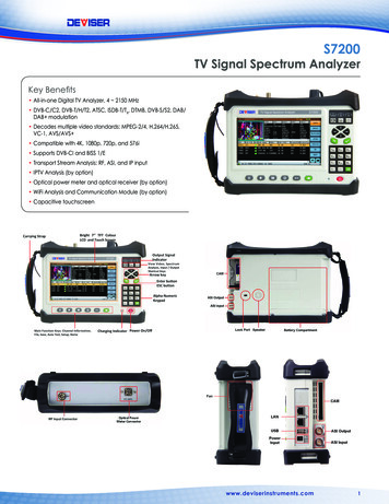
Transcription
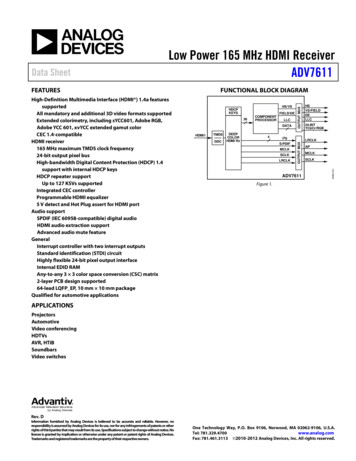
MI1TMDSDDCDEEPCOLORHDMI n Multimedia Interface (HDMI ) 1.4a featuressupportedAll mandatory and additional 3D video formats supportedExtended colorimetry, including sYCC601, Adobe RGB,Adobe YCC 601, xvYCC extended gamut colorCEC 1.4-compatibleHDMI receiver165 MHz maximum TMDS clock frequency24-bit output pixel busHigh-bandwidth Digital Content Protection (HDCP) 1.4support with internal HDCP keysHDCP repeater supportUp to 127 KSVs supportedIntegrated CEC controllerProgrammable HDMI equalizer5 V detect and Hot Plug assert for HDMI portAudio supportSPDIF (IEC 60958-compatible) digital audioHDMI audio extraction supportAdvanced audio mute featureGeneralInterrupt controller with two interrupt outputsStandard identification (STDI) circuitHighly flexible 24-bit pixel output interfaceInternal EDID RAMAny-to-any 3 3 color space conversion (CSC) matrix2-layer PCB design supported64-lead LQFP EP, 10 mm 10 mm packageQualified for automotive applicationsFUNCTIONAL BLOCK DIAGRAMOUTPUT MUXFEATURESOUTPUT MUXData SheetLow Power 165 MHz HDMI ReceiverADV7611Figure 1.APPLICATIONSProjectorsAutomotiveVideo conferencingHDTVsAVR, HTiBSoundbarsVideo switchesRev. DInformation furnished by Analog Devices is believed to be accurate and reliable. However, noresponsibility is assumed by Analog Devices for its use, nor for any infringements of patents or otherrights of third parties that may result from its use. Specifications subject to change without notice. Nolicense is granted by implication or otherwise under any patent or patent rights of Analog Devices.Trademarks and registered trademarks are the property of their respective owners.One Technology Way, P.O. Box 9106, Norwood, MA 02062-9106, U.S.A.Tel: 781.329.4700www.analog.comFax: 781.461.3113 2010-2012 Analog Devices, Inc. All rights reserved.
ADV7611Data SheetTABLE OF CONTENTSFeatures . 1Power-Up Sequence . 10Applications . 1Power-Down Sequence . 10Functional Block Diagram . 1Functional Overview. 11Revision History . 2HDMI Receiver. 11General Description . 3Component Processor . 11Detailed Functional Block Diagram . 3Other Features . 11Specifications. 4Pixel Input/Output Formatting . 12Electrical Characteristics . 4Pixel Data Output Modes Features . 12Data and I C Timing Characteristics . 5Outline Dimensions . 14Absolute Maximum Ratings. 7Ordering Guide . 14Package Thermal Performance . 7Automotive Products . 142ESD Caution . 7Pin Configuration and Function Descriptions . 8Power Supply Sequencing . 10REVISION HISTORY6/12—Rev. C to Rev. DChange to Pin 1 Description, Table 4 . 85/12—Rev. B to Rev. CChanges to Features Section. 1Changes to General Description Section . 3Added Endnote 3 (Table 1) . 4Deleted TDM Serial Timing Parameter (Table 2) . 5Deleted Figure 6 . 7Changed Pin 48 Description (Table 4) . 9Changes to HDMI Receiver and Other Features Sections . 11Added Endnote 1 in Pixel Input/Output Formatting Section andEndnote 1 to Table 5 . 12Deleted Time-Division Multiplexed (TDM) Mode Sectionand Figure 9 . 13Changes to P14 (Table 6) . 13Changes to Ordering Guide . 14Added HDMI Note. 166/11—Rev. A to Rev. BChanges to Figure 7 . 15/11—Rev. 0 to Rev. AChanges to Features Section. 1Changes to Ordering Guide . 16Added Automotive Products Section . 1611/10—Revision 0: Initial VersionRev. D Page 2 of 16
Data SheetADV7611GENERAL DESCRIPTIONThe following audio formats are accessible:The ADV7611 is offered in automotive, professional (noHDCP), and industrial versions. The operating temperaturerange is 40oC to 85oC. The UG-180 contains critical information that must be used inconjunction with the ADV7611.The ADV7611 is a high quality, single input HDMI -capablereceiver. It incorporates an HDMI-capable receiver thatsupports all mandatory 3D TV defined in HDMI 1.4a. TheADV7611 supports formats up to UXGA 60 Hz at 8 bit. A stream from the I2S serializer (two audio channels)A stream from the S/PDIF serializer (two uncompressedchannels or N compressed channels, for example, AC3)DST streamThe HDMI port has dedicated 5 V detect and Hot Plug assertpins. The HDMI receiver also includes an integrated equalizerthat ensures the robust operation of the interface with long cables.It integrates a CEC controller that supports the capabilitydiscovery and control (CDC) feature.The ADV7611 has an audio output port for the audio dataextracted from the HDMI stream. The HDMI receiver has anadvanced mute controller that prevents audible extraneousnoise in the audio output.The ADV7611 contains one main component processor (CP),that processes the video signals from the HDMI receiver. Itprovides features such as contrast, brightness and saturationadjustments, STDI detection block, free run, and synchronizationalignment controls.Fabricated in an advanced CMOS process, the ADV7611 isprovided in a 10 mm 10 mm, 64-lead surface-mount LQFP EP,RoHS-compliant package and is specified over the 40 C to 85 C temperature range.DETAILED FUNCTIONAL BLOCK DIAGRAMCECRXA 5VHPA A/INT2*DDCA SDADDCA SCLRXA C RXA 0 RXA 1 RXA 2 CECCONTROLLERCONTROLINTERFACEI2CCONTROLAND DATA5V DETECTAND ERHDCPENGINE121212ABCDATAPREPROCESORAND OCESSORMUTEAUDIOPROCESSORADV7611*INT2 CAN BE ONLY OUTPUT ON ONE OF THE PINS: SCLK/INT2, MCLK/INT2, OR HPA A/INT2.Figure 2. Detailed Functional Block DiagramRev. D Page 3 of 16P0 TO P7P8 TO P15P16 TO CLK/INT2*09305-002SCLSDAOUTPUT FORMATTERDPLLAUDIO OUTPUT FORMATTERXTALPXTALN
ADV7611Data SheetSPECIFICATIONSAt DVDD 1.71 V to 1.89 V, DVDDIO 3.14 V to 3.46 V, PVDD 1.71 V to 1.89 V, TVDD 3.14 V to 3.46 V, CVDD 1.71 V to 1.89 V,TMIN to TMAX 40 C to 85 C, unless otherwise noted.ELECTRICAL CHARACTERISTICSTable 1.ParameterDIGITAL INPUTS 1Input High VoltageInput Low VoltageInput CurrentInput CapacitanceDIGITAL INPUTS (5 V TOLERANT)1, 2Input High VoltageInput Low VoltageInput CurrentDIGITAL OUTPUTS1Output High VoltageOutput Low VoltageHigh Impedance LeakageCurrentOutput CapacitancePOWER REQUIREMENTS 3, 4Digital Core Power SupplyDigital I/O Power SupplyPLL Power SupplyTerminator Power SupplyComparator Power SupplyDigital Core Supply CurrentDigital I/O Supply CurrentPLL Supply CurrentTerminator Supply CurrentComparator Supply CurrentPOWER-DOWN CURRENTS3, 5Digital Core Supply CurrentDigital I/O Supply CurrentPLL Supply CurrentTerminator Supply CurrentComparator Supply CurrentPower-Up TimeSymbolTest Conditions/CommentsMinVIHVIHVILVILIINXTALN and XTALPOther digital inputsXTALN and XTALPOther digital inputsRESET pinOther digital inputs1.22Typ 45 10CINVIHVILIIN2.6VOHVOLILEAK2.4 82VS/FIELD/ALSB pin 35HPA A/INT2 pinOther10IDVDD PDIDVDDIO PDIPVDD PDITVDD PDICVDD PDtPWRUP1.713.141.713.141.71UXGA 60 Hz at 8 bitUXGA 60 Hz at 8 bitUXGA 60 Hz at 8 bitUXGA 60 Hz at 8 bitUXGA 60 Hz at 8 bitPower-Down Mode 1Power-Down Mode 1Power-Down Mode 1Power-Down Mode 1Power-Down Mode 1Unit0.40.8 6010VVVVµAµApF0.8 82VVµA0.4 60VVµA DDMaxData guaranteed by characterization.The following pins are 5 V tolerant: DDCA SCL, DDC SDA, and RXA 5V.Data recorded during lab characterization.4Maximum current consumption values are recorded with maximum rated voltage supply levels, MoireX video pattern, and at maximum rated temperature.5Power-Down Mode 0 (IO map, Register 0x0C 0x62), ring oscillator powered down (HDMI map, Register 0x48 0x01), and DDC pads off (HDMI map, Register 0x73 0x01).123Rev. D Page 4 of 16
Data SheetADV7611DATA AND I2C TIMING CHARACTERISTICSTable 2.ParameterCLOCK AND CRYSTALCrystal Frequency, XTALPCrystal Frequency StabilityLLC Frequency Range12I C PORTSSCL FrequencySCL Minimum Pulse Width High2SCL Minimum Pulse Width Low2Start Condition Hold Time2Start Condition Setup Time2SDA Setup Time2SCL and SDA Rise Time2SCL and SDA Fall Time2Stop Condition Setup Time2RESET FEATUREReset Pulse WidthCLOCK OUTPUTSLLC Mark-Space Ratio2DATA AND CONTROL OUTPUTS3Data Output Transition Time2, 4I2S PORT, MASTER MODESCLK Mark-Space Ratio2LRCLK Data Transition Time2LRCLK Data Transition Time2I2S Data Transition Time2, 5I2S Data Transition Time2, 5SymbolTest Conditions/CommentsMinTypMaxUnit 55End of valid data to negative clock edgeNegative clock edge to start of valid μsnsnsnsnsnsμs6001.36006001001.00.045:55End of valid data to negative SCLK edgeNegative SCLK edge to start of valid dataEnd of valid data to negative SCLK edgeNegative SCLK edge to start of valid data1Maximum LLC frequency is limited by the clock frequency of UXGA 60 Hz at 8 bit.Data guaranteed by characterization.With the DLL block on output clock bypassed.4DLL bypassed on clock path.5 2I S is accessible via the AP pin.23Rev. D Page 5 of 1655:45% dutycycle2.20.3nsns55:45% dutycyclensnsnsns101055
ADV7611Data SheetTiming Diagramst3t5t3SDAt6t1t7t2t409305-003SCLt82Figure 3. I C Timingt9t10LLCt1109305-004t12P0 TO P23, HS,VS/FIELD/ALSB, DEFigure 4. Pixel Port and Control SDR Output BMSB – 1t20I2SI2S MODEI2SRIGHT-JUSTIFIEDMODEt19MSBMSB – 1t20t19MSBLSBt20NOTES1. I2S IS A SIGNAL ACCESSIBLE VIA THE AP PIN.Figure 5. I2S TimingRev. D Page 6 of 1609305-005I2S
Data SheetADV7611ABSOLUTE MAXIMUM RATINGSPACKAGE THERMAL PERFORMANCETable 3.ParameterDVDD to GNDPVDD to GNDDVDDIO to GNDCVDD to GNDTVDD to GNDDigital Inputs Voltage to GND5 V Tolerant Digital Inputs toGND1Digital Outputs Voltage to GNDXTALP, XTALNSCL/SDA Data Pins to DVDDIOMaximum Junction Temperature(TJ MAX)Storage Temperature RangeInfrared Reflow Soldering (20 sec)1To reduce power consumption when using the ADV7611, theuser is advised to turn off the unused sections of the part.Rating2.2 V2.2 V4.0 V2.2 V4.0 VGND 0.3 V to DVDDIO 0.3 V5.3 VDue to the printed circuit board (PCB) metal variation, and,therefore, variation in PCB heat conductivity, the value of θJAmay differ for various PCBs.GND 0.3 V to DVDDIO 0.3 VGND 0.3 V to PVDD 0.3 VDVDDIO 0.3 V to DVDDIO 3.6 V125 CThe maximum junction temperature (TJ MAX) of 125 C must not beexceeded. The following equation calculates the junction temperature using the measured package surface temperature and appliesonly when no heat sink is used on the device under test (DUT): 60 C to 150 C260 Cwhere:TS is the package surface temperature ( C).ΨJT 0.4 C/W for the 64-lead LQFP EP.The following inputs are 3.3 V inputs but are 5 V tolerant: DDCA SCL andDDCA SDA.Stresses above those listed under Absolute Maximum Ratingsmay cause permanent damage to the device. This is a stressrating only; functional operation of the device at these or anyother conditions above those indicated in the operationalsection of this specification is not implied. Exposure to absolutemaximum rating conditions for extended periods may affectdevice reliability.The most efficient measurement solution is obtained using thepackage surface temperature to estimate the die temperaturebecause this eliminates the variance associated with the θJA value.(TJ TS Ψ JT WTOTAL)WTOTAL ((PVDD IPVDD) (0.05 TVDD ITVDD) (CVDD ICVDD) (DVDD IDVDD) (DVDDIO IDVDDIO))where 0.05 is 5% of the TVDD power that is dissipated on thepart itself.ESD CAUTIONRev. D Page 7 of 16
ADV7611Data DXTALPXTALNDVDDCECDDCA SCLDDCA SDARXA 5VPIN CONFIGURATION AND FUNCTION DESCRIPTIONS64 63 62 61 60 59 58 57 56 55 54 53 52 51 50 4948AP47VS/FIELD/ALSB346HSRXA C 445DETVDD544DVDDIORXA 0–643P0RXA 0 742P1TVDD841P2RXA 1–940DVDDRXA 1 1039P3TVDD 1138P4RXA 2– 1237P5RXA 2 1336P6CVDD 1435P7P23 1534DVDDIOP22 1633P8HPA A/INT21CVDD2RXA C–PIN 1INDICATORADV7611TOP VIEW(Not to Scale)P10P909305-008NOTES1. CONNECT EXPOSED PAD (PIN0) TO GROUND 20P2117 18 19 20 21 22 23 24 25 26 27 28 29 30 31 32Figure 6. Pin ConfigurationTable 4. Pin Function DescriptionsPin No.01MnemonicGNDHPA A/INT2TypeGroundMiscellaneous XA C RXA C TVDDRXA 0 RXA 0 TVDDRXA 1 RXA 1 TVDDRXA 2 RXA 2 CVDDP23P22P21P20P19P18P17P16DVDDIODVDDPowerHDMI inputHDMI inputPowerHDMI inputHDMI inputPowerHDMI inputHDMI inputPowerHDMI inputHDMI inputPowerDigital video outputDigital video outputDigital video outputDigital video outputDigital video outputDigital video outputDigital video outputDigital video outputPowerPowerDescriptionGround.A dual function pin that can be configured to output a Hot Plug assert signal (forHDMI Port A) or an Interrupt 2 signal. This pin is 5 V tolerant.HDMI Analog Block Supply Voltage (1.8 V).Digital Input Clock Complement of Port A in the HDMI Interface.Digital Input Clock True of Port A in the HDMI Interface.Terminator Supply Voltage (3.3 V).Digital Input Channel 0 Complement of Port A in the HDMI Interface.Digital Input Channel 0 True of Port A in the HDMI Interface.Terminator Supply Voltage (3.3 V).Digital Input Channel 1 Complement of Port A in the HDMI Interface.Digital Input Channel 1 True of Port A in the HDMI Interface.Terminator Supply Voltage (3.3 V).Digital Input Channel 2 Complement of Port A in the HDMI Interface.Digital Input Channel 2 True of Port A in the HDMI Interface.HDMI Analog Block Supply Voltage (1.8 V).Video Pixel Output Port.Video Pixel Output Port.Video Pixel Output Port.Video Pixel Output Port.Video Pixel Output Port.Video Pixel Output Port.Video Pixel Output Port.Video Pixel Output Port.Digital I/O Supply Voltage (3.3 V).Digital Core Supply Voltage (1.8 V).Rev. D Page 8 of 16
Data SheetADV7611Pin DDP2P1P0DVDDIODEHSVS/FIELD/ALSBTypeDigital video outputDigital video outputDigital video outputDigital video outputDigital video outputDigital video outputDigital video outputDigital video outputDigital video outputPowerDigital video outputDigital video outputDigital video outputDigital video outputDigital video outputPowerDigital video outputDigital video outputDigital video outputPowerMiscellaneous digitalDigital video outputDigital input/output48APMiscellaneous digital49SCLK/INT2Miscellaneous digital5051LRCLKMCLK/INT2Miscellaneous digitalMiscellaneous digital52535455DVDDSCLSDAINT1PowerMiscellaneous digitalMiscellaneous digitalMiscellaneous digital56RESETMiscellaneous digital5758PVDDXTALPPowerMiscellaneous analog596061626364XTALNDVDDCECDDCA SCLDDCA SDARXA 5VMiscellaneous analogPowerDigital input/outputHDMI inputHDMI inputHDMI inputDescriptionLine-Locked Output Clock for the Pixel Data (Range is 13.5 MHz to 162.5 MHz).Video Pixel Output Port.Video Pixel Output Port.Video Pixel Output Port.Video Pixel Output Port.Video Pixel Output Port.Video Pixel Output Port.Video Pixel Output Port.Video Pixel Output Port.Digital I/O Supply Voltage (3.3 V).Video Pixel Output Port.Video Pixel Output Port.Video Pixel Output Port.Video Pixel Output Port.Video Pixel Output Port.Digital Core Supply Voltage (1.8 V).Video Pixel Output Port.Video Pixel Output Port.Video Pixel Output Port.Digital I/O Supply Voltage (3.3 V).DE (data enable) is a signal that indicates active pixel data.HS is a horizontal synchronization output signal.VS is a vertical synchronization output signal. FIELD is a field synchronization outputsignal in all interlaced video modes. VS or FIELD can be configured for this pin. TheALSB allows selection of the I2C address.Audio Output Pin. Pin can be configured to output S/PDIF digital audio output(S/PDIF) or I2S.A dual function pin that can be configured to output an audio serial clock or anInterrupt 2 signal.Audio Left/Right Clock.A dual function pin that can be configured to output an audio master clock or anInterrupt 2 signal.Digital Core Supply Voltage (1.8 V).I2C Port Serial Clock Input. SCL is the clock line for the control port.I2C Port Serial Data Input/Output Pin. SDA is the data line for the control port.Interrupt. This pin can be active low or active high. When status bits change, this pin istriggered. The events that trigger an interrupt are under user configuration.System Reset Input. Active low. A minimum low reset pulse width of 5 ms is requiredto reset the ADV7611 circuitry.PLL Supply Voltage (1.8 V).Input Pin for 28.63636 MHz Crystal or an External 1.8 V, 28.63636 MHz Clock OscillatorSource to Clock the ADV7611.Crystal Input. Input pin for 28.63636 MHz crystal.Digital Core Supply Voltage (1.8 V).Consumer Electronic Control Channel.HDCP Slave Serial Clock Port A. DDCA SCL is a 3.3 V input that is 5 V tolerant.HDCP Slave Serial Data Port A. DDCA SDA is a 3.3 V input that is 5 V tolerant.5 V Detect Pin for Port A in the HDMI Interface.Rev. D Page 9 of 16
ADV7611Data SheetPOWER SUPPLY SEQUENCINGThe recommended power-up sequence of the ADV7611 is topower up the 3.3 V supplies first, followed by the 1.8 V supplies.Reset should be held low while the supplies are powered up.Alternatively, the ADV7611 may be powered up by asserting allsupplies simultaneously. In this case, care must be taken while thesupplies are being established to ensure that a lower rated supplydoes not go above a higher rated supply level.POWER SUPPLY (V)POWER-UP SEQUENCE3.3V3.3V SUPPLIES1.8V1.8V SUPPLIESThe ADV7611 supplies may be deasserted simultaneously aslong as a higher rated supply does not go below a lower ratedsupply.3.3V SUPPLIESPOWER-UP1.8V SUPPLIESPOWER-UPFigure 7. Recommended Power-Up SequenceRev. D Page 10 of 1609305-007POWER-DOWN SEQUENCE
Data SheetADV7611FUNCTIONAL OVERVIEWHDMI RECEIVERCOMPONENT PROCESSORThe receiver supports all mandatory and many optional 3Dformats. It supports HDTV formats up to UXGA at 8 bit.The ADV7611 has an any-to-any 3 3 CSC matrix. The CSCblock is placed at the back of the CP section. CSC enablesYPrPb-to-RGB and RGB-to-YCrCb conversions. Many otherstandards of color space can be implemented using the colorspace converter.The HDMI-compatible receiver on the ADV7611 incorporatesprogrammable equalization of the HDMI data signals. Thisequalization compensates for the high frequency losses inherentin HDMI and DVI cabling, especially at longer lengths and higherfrequencies. It is capable of equalizing for cable lengths up to30 meters to achieve robust receiver performance.With the inclusion of HDCP, displays can receive encryptedvideo content. The HDMI interface of the ADV7611 allows forauthentication of a video receiver, decryption of encoded dataat the receiver, and renewability of that authentication duringtransmission, as specified by the HDCP 1.4 protocol.The ADV7611 has a synchronization regeneration block usedto regenerate the DE based on the measurement of the videoformat being displayed and to filter the horizontal and verticalsynchronization signals to prevent glitches. The HDMI receiveralso supports TERC4 error detection, used for detection ofcorrupted HDMI packets following a cable disconnect.The HDMI receiver contains an audio mute controller thatcan detect a variety of conditions that may result in audibleextraneous noise in the audio output. On detection of theseconditions, the audio signal can be ramped to prevent audioclicks or pops. Audio output can be formatted to LPCM andIEC 61937.The HDMI receiver features include: 162.5 MHz (UXGA at 8 bit) maximum TMDS clockfrequency3D format support defined in HDMI 1.4a specificationIntegrated equalizer for cable lengths up to 30 metersHDCP 1.4Internal HDCP keysPCM audio packet supportRepeater supportInternal EDID RAMHot Plug assert output pin for an HDMI portCEC controllerCP features include: 525i, 625i, 525p, 625p, 720p, 1080i, 1080p, and otherformatsManual adjustments including gain (contrast) andoffset (brightness), hue, and saturationFree run output mode that provides stable timing when novideo input is present162.5 MHz processing rateContrast, brightness, hue, and saturation controlsStandard identification enabled by STDI blockRGB that can be color space converted to YCrCb anddecimated to a 4:2:2 format for video-centric back end ICinterfacingDE output signal supplied for direct connection to anHDMI/DVI transmitterOTHER FEATURESThe ADV7611 has HS, VS, FIELD, and DE output signals withprogrammable position, polarity, and width.The ADV7611 has programmable interrupt request output pins,including INT1 and INT2 (INT2 is accessible only via one offollowing pins: MCLK/INT2, SCLK/INT2, or HPA A/INT2).It also features a low power-down mode. The I2C address ofthe main map is 0x98 after reset. This can be changed after resetto 0x9A if pullup is attached to VS/FIELD/ALSB pin and I2Ccommand SAMPLE ALSB is issued. Refer to the RegisterAccess and Serial Ports Description section in the UG-180.The ADV7611 is provided in a 10 mm 10 mm, RoHS-compliantLQFP EP package, and is specified over the 40 C to 85 Ctemperature range.Rev. D Page 11 of 16
ADV7611Data SheetPIXEL INPUT/OUTPUT FORMATTINGThe output section of the ADV7611 is highly flexible. The pixeloutput bus can support up to 24-bit 4:4:4 YCrCb. The pixel datasupports both single and double data rates modes. In SDR mode, a16-/24-bit 4:2:2 or 24-bit 4:4:4 output is possible. In DDR mode 1,the pixel output port can be configured in an 8-/12-bit 4:2:2 YCrCbor 24-bit 4:4:4 RGB.Bus rotation is supported. Table 5 and Table 6 outline the differentoutput formats that are supported. All output modes are controlledvia I2C.1DDR mode is only supported only up to 50 MHz (an equivalent to data rateclocked 100 MHz clock in SDR mode).PIXEL DATA OUTPUT MODES FEATURESThe output pixel port features include: 8-/12-bit ITU-R BT.656 4:2:2 YCrCb with embedded timecodes and/or HS, VS, and FIELD output signals16-/24-bit YCrCb with embedded time codes and/or HSand VS/FIELD pin timing24-bit YCrCb/RGB with embedded time codes and/or HSand VS/FIELD pin timingDDR 8-/12-bit 4:2:2 YCrCbDDR 24-bit 4:4:4 RGBTable 5. SDR 4:2:2 and 4:4:4 Output ModesOP FORMAT SEL[7:0]Pixel P8P7P6P5P4P3P2P1P010x08-Bit SDRITU-R BT.656Mode 7, Cb7, Cr7Y6, Cb6, Cr6Y5, Cb5, Cr5Y4, Cb4, Cr4Y3, Cb3, Cr3Y2, Cb2, Cr2Y1, Cb1, Cr1Y0, Cb0, Z10x0A12-Bit SDRITU-R BT.656Mode 2Y3, Cb3, Cr3Y2, Cb2, Cr2Y1, Cb1, Cr1Y0, Cb0, Cr0High-ZHigh-ZHigh-ZHigh-ZY11, Cb11, Cr11Y10, Cb10, Cr10Y9, Cb9, Cr9Y8, Cb8, Cr8Y7, Cb7, Cr7Y6, Cb6, Cr6Y5, Cb5, Cr5Y4, Cb4, Z1SDR 4:2:20x8016-Bit SDRITU-R BT.656 4:2:2Mode 7Y6Y5Y4Y3Y2Y1Y0Cb7, Cr7Cb6, Cr6Cb5, Cr5Cb4, Cr4Cb3, Cr3Cb2, Cr2Cb1, Cr1Cb0, Cr00x8A24-Bit SDRITU-R BT.656 4:2:2Mode 2Y3Y2Y1Y0Cb3, Cr3Cb2, Cr2Cb1, Cr1Cb0, Cr0Y11Y10Y9Y8Y7Y6Y5Y4Cb11, Cr11Cb10, Cr10Cb9, Cr9Cb8, Cr8Cb7, Cr7Cb6, Cr6Cb5, Cr5Cb4, Cr4Modes 0x00 and 0x0A require additional writes to IO Map Register 0x19[7:6] 2’b11 and IO Map Register 0x33[6] 1Rev. D Page 12 of 16SDR 4:4:40x4024-Bit SDR 4:4:4Mode 0R7R6R5R4R3R2R1R0G7G6G5G4G3G2G1G0B7B6B5B4B3B2B1B0
Data SheetADV7611Table 6. DDR 4:2:2 and 4:4:4 Output ModesOP FORMAT SEL[7:0]Pixel P8P7P6P5P4P3P2P1P012DDR 4:2:2 Mode (Clock/2)0x208-Bit DDR ITU-656(Clock/2 Output) 4:2:2 Mode 0Clock RiseClock Cb7, Cr7Y7Cb6, Cr6Y6Cb5, Cr5Y5Cb4, Cr4Y4Cb3, Cr3Y3Cb2, Cr2Y2Cb1, Cr1Y1Cb0, ZDDR 4:2:2 Mode (Clock/2)0x2A12-Bit DDR ITU-656(Clock/2 Output) 4:2:2 Mode 2Clock RiseClock FallCb3, Cr3Y3Cb2, Cr2Y2Cb1, Cr1Y1Cb0, h-ZCb11, Cr11Y11Cb10, Cr10Y10Cb9, Cr9Y9Cb8, Cr8Y8Cb7, Cr7Y7Cb6, Cr6Y6Cb5, Cr5Y5Cb4, Z-0 even samples.-1 odd samples.Rev. D Page 13 of 16DDR 4:4:4 Mode (Clock/2) 1, 20x6024-Bit DDR RGB(Clock/2 Output)Clock RiseClock -0B5-1B4-0B4-1B3-0B3-1B2-0B2-1B1-0B1-1B0-0B0-1
ADV7611Data SheetOUTLINE DIMENSIONS0.750.600.4512.2012.00 SQ11.801.60MAX10.2010.00 SQ9.804949644811.00 REF64148PIN 1SEATINGPLANEEXPOSEDPAD5.105.00 SQ4.907.50REF SQBOTTOM VIEWTOP VIEW0.200.090.150.057 0 (PINS DOWN)1633321716331732VIEW A0.08COPLANARITY0.50LEAD PITCHVIEW AROTATED 90 CCWCOMPLIANT TO JEDEC STANDARDS MS-026-BCD-HD0.270.220.17FOR PROPER CONNECTION OFTHE EXPOSED PAD, REFER TOTHE PIN CONFIGURATION ANDFUNCTION DESCRIPTIONSSECTION OF THIS DATA SHEET.06-12-2012-A1.451.401.35(PINS UP)Figure 8. 64-Lead Low Profile Quad Flat Package (LQFP EP)SW-64-2Dimensions shown in millimetersORDERING GUIDEModel 1, AL-ADV7611EB2ZNotes3433Temperature Range 40 C to 85 C 40 C to 85 C 40 C to 85 C 40 C to 85 C 40 C to 85 C 40 C to 85 CPackage Description64-Lead LQFP EP64-Lead LQFP EP64-Lead LQFP EP64-Lead LQFP EP64-Lead LQFP EP64-Lead LQFP EPEvaluation Board with HDCP KeysEvaluation Board Without HDCP KeysPackage OptionSW-64-2SW-64-2SW-64-2SW-64-2SW-64-2SW-64-2Z RoHS Compliant Part.W Qualified for Automotive Parts.313” Tape and Reel.4Non-HDCP version.12AUTOMOTIVE PRODUCTSThe ADV7611W models are available with controlled manufacturing to support the quality and reliability requirements of automotiveapplications. Note that these automotive models may have specifications that differ from the commercial models; therefore, designersshould review the Specifications section of this data sheet carefully. Only the automotive grade products shown are available for use inautomotive applications. Contact your local Analog Devices, Inc., account representative for specific product ordering information and toobtain the specific Automotive Reliability report for this model.Rev. D Page 14 of 16
Data SheetADV7611NOTESRev. D Page 15 of 16
ADV7611Data SheetNOTESHDMI, the HDMI Logo, and High-Definition Multimedia Interface are trademarks or registered trademarks of HDMI Licensing LLC in the United States and othercountries. 2010-2012 Analog Devices, Inc. All rights reserved. Trademarks andregistered trademarks are the property of their respective owners.D09305-0-6/12(D)Rev. D Page 16 of 16
video conferencing . hdtvs . avr, htib . soundbars . video switches . functional block diagram hs/vs 4 i 2 s s/pdif hdcp keys tmds ddc hdmi1 deep color hdmi rx adv7611 component 36 processor output mux field/de llc mclk sclk lrclk lrclk ap mclk output mux sclk 24-bit ycbcr/rgb hs vs/field de llc 09305-001. figure 1.