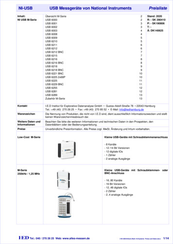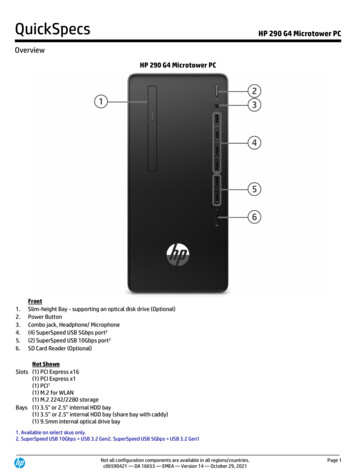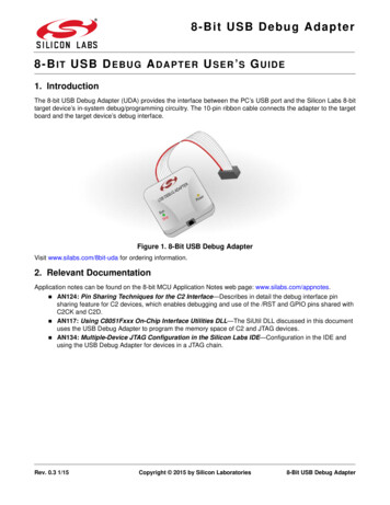
Transcription
JMS561JMS561SuperSpeed USBtoDual SATA Gen3 PortsBridgePreliminary DatasheetRevision 1.0.1Revision 1.0.1 JMicron 2014. All rights reserved.Page 1Copying prohibited.
JMS561Revision HistoryVersionDateRevision Descriptionyyyy/mm/dd1. Correct 1.1.1 typo2. Correct “XIN” description1.0.12014/04/203. Correct “XOUT” description4. Correct “VREG-IN” description5. Correct “FB” description6. Correct Reset Timing1.0.02013/10/31 Release revision 1.0.0Revision 1.0.1 JMicron 2014. All rights reserved.Page 2Copying prohibited.
JMS561 Copyright JMicron Technology 2014.All Rights Reserved.Printed in Taiwan 2014JMicron and the JMicron Logo are trademarks of JMicron Technology Corporation in Taiwan and/or other countries.Other company, product and service names may be trademarks or service marks of others.All information contained in this document is subject to change without notice. The products described in thisdocument are NOT intended for use implantation or other life supports application where malfunction may result ininjury or death to persons. The information contained in this document does not affect or change JMicron’sproduct specification or warranties. Nothing in this document shall operate as an express or implied license orenvironments, and is presented as an illustration. The results obtained in other operating environments may vary.THE INFORMATION CONTAINED IN THIS DOCUMENT IS PROVIEDE ON AN “AS IS” BASIS. In no event willJMicron be liable for damages arising directly or indirectly from any use of the information contained in thisdocument.JMicron Technology Corporation1F, No.13, Innovation Road 1,Hsinchu Science Park,Hsinchu, Taiwan, R.O.CFor more information on JMicron products, please visit the JMicron website athttp://www.JMicron.com or send email to sales@jmicron.comRevision 1.0.1 JMicron 2014. All rights reserved.Page 3Copying prohibited.
JMS561Table of Contents1.2.3.4.5.Overviews .51.1FUNCTION OVERVIEW .51.1.1 FEATURES .51.1.2 BLOCK DIAGRAM .61.2SUPPORT DEVICES .71.3APPLICATION EXAMPLES .71.3.1 USB 2.0 and USB 3.0 to two SATA Gen3 HDDs .71.3.2 USB 2.0, USB 3.0 and eSATA 6G to one SATA Gen3 HDD .7Package Pin-Out .82.1PIN TYPE DEFINITION .92.2PIN DESCRIPTION .9External SPI Flash.13Clock & Reset.144.1Crystal input .144.2Reset input .14Electrical Characteristics .155.15.25.35.46.Absolute Maximum Rating .15Recommended Power Supply Operation Conditions .15Recommended External Clock Source Conditions .15Power Supply DC Characteristics .165.4.1 USB2.0 to SATAx2 mode .165.4.2 USB3.0 to SATAx2 mode .175.5I/O DC Characteristics .175.6Power-On Sequence .18Internal Switch Regulator .207.8.Performance Benchmark .21Package Dimension .22Revision 1.0.1 JMicron 2014. All rights reserved.Page 4Copying prohibited.
JMS5611. Overviews1.1 FUNCTION OVERVIEW1.1.1 FEATURES Complies with Serial ATA International Organization: Serial ATA Revision 3.1 Complies with Universal Serial Bus 3.0 Specification Revision 1.0 Complies with USB Mass Storage Class Bulk-Only Transport (BOT) Rev. 1.0 Specification Complies with USB Attached SCSI Protocol (UASP) Rev. 1.0 Specification Supports USB Super-Speed/High-Speed/Full-Speed Operation Supports USB 2.0/USB 3.0 power saving mode Supports multi LUNs for USB 2.0/USB 3.0 Supports port multiplier for eSATA Supports hardware RAID0 (striping) and RAID1 (mirror) over USB 2.0/USB 3.0/eSATA Flexible GPIOs for customized functions Provides a hardware control PWM Provides software utilities for downloading the upgraded firmware code under USB2.0/USB3.0/eSATA Design for Windows XP, Windows 7, Windows 8, MAC 10.3 or later versions 30MHz external crystal An embedded 3.3V to 1.2V voltage regulator An embedded 5.0V to 3.3V voltage regulator QFN 64 packageRevision 1.0.1 JMicron 2014. All rights reserved.Page 5Copying prohibited.
JMS561USB 3.0MAC8051Switch VRSATA MACPeripheralControllerSRAMSATA Gen3PHYUSB 3.0SATA MACSPISATA Gen3PHYUSB 2.0 PHYUSB 2.0MACSRAMUSB 2.0USB 3.0 PHY1.1.2 BLOCK DIAGRAMSATA Gen3SPI FlashSATA Gen3VIA ROMJMS561Revision 1.0.1 JMicron 2014. All rights reserved.Page 6Copying prohibited.
JMS5611.2 SUPPORT DEVICES Hard disk drives1.3 APPLICATION EXAMPLES1.3.1 USB 2.0 and USB 3.0 to two SATA Gen3 HDDsSATA Gen3USB 2.0USB 3.0561SATA Gen31.3.2 USB 2.0, USB 3.0 and eSATA 6G to one SATA Gen3 HDDUSB 2.0SATA Gen3USB 3.0561eSATA 6GRevision 1.0.1 JMicron 2014. All rights reserved.Page 7Copying prohibited.
JMS561S0 RXP38AVDDHS0 RXN3933AVDDL40XOUTS0 TXN41XINS0 TXP4234AVDDH4335S1 RXP44AVDDLS1 RXN45AUX-REXTAVDDL4636S1 TXN4737S1 TXP482. Package Pin-OutGPIO17/TACH-IN4932AVDDLGPIO9/D0 PWR CNTL5031SSRXPVCCK5130SSRXNVCCO5229AVDDLGPIO10/D0 ERR LED25328SSTXPRST#5427SSTXNGPIO11/D0 ACT 3DMVREG-GND5922LDO 3V OUTVREG-OUT6021LDO 5V PIO2/P-SPI-CEFB6417VCCKRevision 1.0.1 JMicron 2014. All rights 4/S-SPI-CKGPIO8/D1 PWR CNTLGPIO14/D1 ERR LED3VCCOGPIO12/D1 ACT -SIVBUS SENSEJMS561Page 8Copying prohibited.
JMS5612.1 PIN TYPE DEFINITIONPin ectionalSInternal Schmitt Trigger Circuit is usedLInternal weak pull-low (Max. 164K , Typical 96 K , Min. 61K )HInternal weak pull-high (Max. 141K , Typical 93 K , Min. 66K )2.2 PIN DESCRIPTIONSignalNameQFN 64TypeDescriptionSerial ATA interfaceS0 RXP38AIS0 RXN39AIS0 TXP42AOS0 TXN41AOS1 RXP44AIS1 RXN45AIS1 TXP48AOS1 TXN47AOREXT36AISATA Port RX Signal.A 10nF capacitor should be connected between this pin andSATA connector.SATA Port RX- Signal.A 10nF capacitor should be connected between this pin andSATA connector.SATA Port TX Signal.A 10nF capacitor should be connected between this pin andSATA connector.SATA Port TX- Signal.A 10nF capacitor should be connected between this pin andSATA connector.SATA Port RX Signal.A 10nF capacitor should be connected between this pin andSATA connector.SATA Port RX- Signal.A 10nF capacitor should be connected between this pin andSATA connector.SATA Port TX Signal.A 10nF capacitor should be connected between this pin andSATA connector.SATA Port TX- Signal.A 10nF capacitor should be connected between this pin andSATA connector.External Reference Resistance.A 12K 1% external resistor should be connected to this pin.USB 3.0 interfaceRevision 1.0.1 JMicron 2014. All rights reserved.Page 9Copying prohibited.
JMS561SignalNameQFN 64TypeSSRXP31AISuper Speed RX Signal.SSRXN30AISuper Speed RX- Signal.SSTXP28AOSSTXN27AOSSREXT25AIDM23AIOUSB 2.0 Bus D- Signal.DP24AIOLDO 5V IN21AILDO 3VOUT22AOUSB 2.0 Bus D Signal.5.0V to 3.3V LDO Power Input.This pin should be connected to the 5V input or USBconnector 5V.Capacitance for internal LDO of USB 2.0.A capacitance to ground is recommended on this pin. Thevalue should be 1uF.The output voltage range is 3.3V 10%.VBUSSENSE16AIDescriptionSuper Speed TX Signal.A 100nF capacitor should be connected between this pin andUSB connector.Super Speed TX- Signal.A 100nF capacitor should be connected between this pin andUSB connector.External Reference Resistance.A 12K 1% external resistor should be connected to this pin.USB 2.0 interfaceUSB 2.0/USB 3.0 Cable Power InputThis pin should be connected to USB connector 5V.Crystal InterfaceXIN35AIXOUT34AOCrystal Input/Oscillator Input.It is connected to a 30MHz crystal or crystal oscillator. Thevariation range should be 30ppm. And the input voltageshould range in 3.3V 5%.Crystal Output.It is connected to a crystal. While crystal oscillator is applied,this pin should be reserved as No Connection (NC). Theoutput variation range is around 30ppm (input dependent).And the output voltage range is 3.3V 5% (input dependent).Switching RegulatorVREG-GND58,59AISwitching Regulator Ground.VREG-OUT60,61AOSwitch Output Pin.An external inductor should be connected to this pin.VREG-IN62,63AISwitching Regulator 3.3V Power Supply.FB64AIFeedback pin which is connected to 1.2V core voltage.Revision 1.0.1 JMicron 2014. All rights reserved.Page 10Copying prohibited.
JMS561SignalNameQFN 64TypeDescriptionControl and GPIOsSystem Global Reset Input.Active-low to reset the entire chip.An external RC should be connected to this pin. Please referto the following section for detailed description.MP Test Mode Enable.This pin is reserved for IC mass production testing.Please set this pin to low under normal operation.8051 UART Output / GPIO [0].This pin only preserves for UART TX OHGPIO [9].This pin only preserves for enable hard drive power.GPIO[10]53DIOHGPIO [10].This pin can be programmed by customized firmware.GPIO[11]55DIOHGPIO [11].This pin can be programmed by customized Revision 1.0.1 JMicron 2014. All rights reserved.8051 UART Input / GPIO [1].This pin only preserves for UART RX function.Primary Serial Flash (CE) / GPIO [2]This pin only preserves for SPI chip enable.GPIO [3].This pin only preserves for FAN function.Secondary Serial Flash (SCK) / GPIO [4]This pin can be programmed as special function or normalGPIO function.Secondary Serial Flash (SO) / GPIO [5]This pin can be programmed as special function or normalGPIO function.Secondary Serial Flash (SI) / GPIO [6]This pin only preserves for UART function.Secondary Serial Flash (CE) / GPIO [7]This pin can be programmed as special function or normalGPIO function.GPIO [8].This pin only preserves for enable hard drive power.GPIO [12].This pin can be programmed by customized firmware.Primary Serial Flash (SI) / GPIO [13]This pin can be programmed as special function or normalGPIO function.GPIO [14].This pin can be programmed by customized firmware.Page 11Copying prohibited.
JMS561SignalNameQFN scriptionPrimary Serial Flash (SCK) / GPIO [15]This pin can be programmed as special function or normalGPIO function.Primary Serial Flash (SO) / GPIO [16]This pin can be programmed as special function or normalGPIO function.GPIO [17].This pin only preserves for FAN TACH In function.Power and GroundVCCO10,52PDigital I/O Power Supply.VCCK4,12,1720,51,57PDigital Core Power Supply.AVDDH26,33,43PAnalog I/O Power Supply.AVDDL29,32,3740,46PAnalog Core Power Supply.LED IndicatorIf user has an application for LED function, please contact JMicron’s AE before PCB layout.GPIO initial valueAll GPIOs set as input mode with pull-high resistor while in reset.Revision 1.0.1 JMicron 2014. All rights reserved.Page 12Copying prohibited.
JMS5613. External SPI FlashVendor NameModel NameMXIC25L400 1EMXIC25L4005 AMCMXIC25L1605 DM2IMXIC25L8005 Giga ion 1.0.1 JMicron 2014. All rights reserved.Page 13CommentCopying prohibited.
JMS5614. Clock & Reset4.1 Crystal inputSingle crystal input at 30MHz is needed.4.2 Reset inputThe reset input pin is the Schmitt trigger input pin. All functions will be initialized by reset except theAnalog Power-On Reset Circuit depending on the Power on-off.Revision 1.0.1 JMicron 2014. All rights reserved.Page 14Copying prohibited.
JMS5615. Electrical Characteristics5.1 Absolute Maximum RatingParameterSymbolConditionMinMaxUnitDigital I/O power supplyVCCO(ABS)-0.33.47VDigital core power supplyVCCK(ABS)-0.31.26VAnalog I/O power supplyAVDDH(ABS)-0.33.47VAnalog core power supplyAVDDL(ABS)-0.31.26VUSB VBUS power supplyVBUS-0.35.5VVI(D)-0.33.47Digital I/O input voltageStorage TemperatureTSTORAGE-40Vo150C5.2 Recommended Power Supply Operation tDigital I/O power supplyVCCO3.133.33.47VDigital core power supplyVCCK1.141.21.26VAnalog I/O power supplyAVDDH3.133.33.47VAnalog core power supplyAVDDL1.141.21.26VVI(D)03.33.47Digital I/O input voltageVAmbient operation temperatureTA070oJunction TemperatureTJ-40125oCC5.3 Recommended External Clock Source ConditionsParameterSymbolConditionMinExternal reference clockMax30Clock Duty CycleRevision 1.0.1 JMicron 2014. All rights reserved.Typical45Page 1550UnitMHz55%Copying prohibited.
JMS5615.4 Power Supply DC CharacteristicsThe maximum and minimum values are measured at the max and min power supply levels respectively.5.4.1 USB2.0 to SATAx2 mode@S0 stateParameter3.3V power supply1.2V power supplySymbolVCCO andACDDHVCCK andAVDDLConditionMinTypicalMaxUnitOperate @3.3V40.548.656.0mAOperate @1.2V325.4328.3332.4mAMinTypicalMaxUnitOperate @3.3V3.03.03.0mAOperate @1.2V4.04.04.1mA@S4 stateParameter3.3V power supply1.2V power supplyRevision 1.0.1 JMicron 2014. All rights reserved.SymbolVCCO andACDDHVCCK andAVDDLConditionPage 16Copying prohibited.
JMS5615.4.2 USB3.0 to SATAx2 mode@U0 stateParameter3.3V power supply1.2V power supplySymbolVCCO andACDDHVCCK andAVDDLConditionMinTypicalMaxUnitOperate @3.3V45.953.961.3mAOperate @1.2V450.6455.4477.7mA@U3 state (suspend @S4)Parameter3.3V power supply1.2V power supplySymbolVCCO andACDDHVCCK andAVDDLConditionMinTypicalMaxUnitOperate @3.3V3.03.03.1mAOperate @1.2V7.07.07.1mAConditionMinMaxUnit0.7V5.5 I/O DC CharacteristicsParameterSymbolInput low voltageVILInput high voltageVIHOutput low voltageVOLOutput high voltageVOHRevision 1.0.1 JMicron 2014. All rights reserved.Typical1.5V0.31.9Page 17VVCopying prohibited.
JMS5615.6 Power-On SequenceThe Power-On sequence rules are defined in this section. Designers should follow all the rules forexternal power designs. Detailed explanations are listed as below.T1VCCO2.0VT3VCCKT20.88VT4RST#2.0VT5T1: Rise time for 3.3V power rail from 0.0V to 3.3VT2: Rise time for 1.2V power rail from 0.0V to 1.2VT3: Rise time for 3.3V power rail from 0.0V to 2.0VT4: Rise time for 1.2V power rail from 0.0V to 0.88VT5: Rise time for RST# signal from 0.0V to 2.0VRevision 1.0.1 JMicron 2014. All rights reserved.Page 18Copying prohibited.
JMS561The recommended power sequence and timing requirements are listed as below.TimeMinimumMaximumT10.0 ms10 msT20.0 ms10 msT30.0 ms8 msT40.0 ms8 msT5100 ms500 msThe RESET timing constrain is based on the external RC reset circuits. In order to control the chargeand discharge time for RC circuits, minimum and maximum requirements are listed. If designers applytiming control chip to control the reset signal, the only requirement will be minimum value. In otherwords, the maximum value can be skipped without problems.Revision 1.0.1 JMicron 2014. All rights reserved.Page 19Copying prohibited.
JMS5616. Internal Switch RegulatorInput Voltage Range: 2.375V 5.500VOutput Voltage Range: 1.0V 1.4 (programmable)Output Voltage Accuracy : ILOAD 650mA, VOUT 10%Max. Output Current : 650mAOver-Current Protection (OCP): Yes (1,500mA)Output Capacitor: 20uFOutput Inductor: 3.3uHStart-up Time : 1.5 msThermal Shutdown: NoFaster Shutdown: NoRevision 1.0.1 JMicron 2014. All rights reserved.Page 20Copying prohibited.
JMS5617. Performance BenchmarkUSB3.0 UAS Performance 400 MB/sUSB2.0 UAS Performance 42 MB/sRevision 1.0.1 JMicron 2014. All rights reserved.Page 21Copying prohibited.
JMS5618. Package Dimension QFN 64 8x8 mm2Revision 1.0.1 JMicron 2014. All rights reserved.Page 22Copying prohibited.
Complies with Serial ATA International Organization: Serial ATA Revision 3.1 Complies with Universal Serial Bus 3.0 Specification Revision 1.0 Complies with USB Mass Storage Class Bulk-Only Transport (BOT) Rev. 1.0 Specification Complies with USB Attached SCSI Protocol (UASP) Rev. 1.0 Specification