Transcription
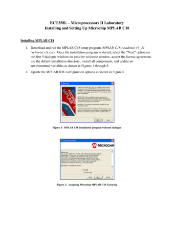
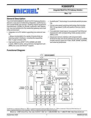
KS8695PXIntegrated Multi-Port PCI Gateway SolutionRev. 1.3General DescriptionThe CENTAUR KS8695PX, Multi-Port PCI Gateway Solution,delivers a new level of networking integration, performance,and overall BOM cost savings, enabling original equipmentmanufacturers (OEMs) to provide customers with featurerich, low-cost solutions for the residential gateway and smalloffice environment. Integration of a PCI arbiter supporting one external master.– Allows incorporation of a variety of productivity enhancing system interfaces, including the expanding802.11 a/g/b wireless LAN. High-performance ARMTM CPU (ARM9) with 8KBI-cache, 8KB D-cache, and a memory management unit(MMU) for Linux and WinCE support. XceleRouterTM technology to accelerate packet processing. Proven wire-speed switching technology that includes802.1Q tag-based VLAN and quality of service (QoS)support. Five patented mixed-signal, low-powered Fast Ethernettransceivers with corresponding media access control(MAC) units. Advanced memory interface with programmable8/16/32-bit data and 22-bit address bus with up to 64MBof total memory space for Flash, ROM, SRAM, SDRAM,and external peripherals.Functional DiagramCENTAUR KS8695PXAdvanced Memory ControllerFLASH/ROM/SRAMControllerExternal I/OControllerSDRAMControllerARM9 MMUHigh Speed AMBA Bus8KBI-CacheAPBBridgeXceleRouter Advanced Peripheral Bus (APB)SwitchRegisters1 ExternalPCI gh-PerformanceNon-Blocking5-Port Switch16 WatchdogXceleRouter is a trademark of Micrel, Inc. AMD is a registered trademark of Advanced Micro Devices, Inc. ARM is a trademark of Advanced RISC Machines Ltd.Intel is a registered trademark of Intel Corporation. WinCE is a registered trademark of Microsoft Corporation.Micrel, Inc. 2180 Fortune Drive San Jose, CA 95131 USA tel 1 (408) 944-0800 fax 1 (408) 474-1000 http://www.micrel.comSeptember 20051M9999-091605
KS8695PXMicrelFeatures Memory and External I/O Interfaces– 8/16/32-bit wide shared data path for Flash, ROM,SRAM, SDRAM, and external I/O– Total memory space up to 64MB– Intel /AMD -type Flash support Peripheral Support– 8/16/32-bit external I/O interface supporting PCMCIAor generic CPU/DSP host I/F– Sixteen general purpose input/output (GPIO)– Two 32-bit timer counters (one watchdog)– Interrupt controller System Design– Up to 166MHz CPU and 125MHz bus speed– 289 PBGA package (19mm x 19mm) saving boardreal estate– Two power supplies: 1.8V core and Ethernet RXsupply, 3.3V I/O and Ethernet TX supply– Built-in LED controls Debugging– ARM9 JTAG debug interface– UART for console port or modem back-up Power Management– CPU and system clock speed step-down options– Low-power Ethernet transceivers– Per port power-down and Ethernet transmit disable Reference Hardware and Software Evaluation Kit– Hardware evaluation board (passes class B EMI)– Board support package including firmware sourcecodes, Linux kernel, and software stacks– Complete hardware and software reference designsavailableThe CENTAUR KS8695PX featuring XceleRouter technologyis a single-chip, multi-port PCI "gateway-on-a-chip" with allthe key components integrated for a high-performance andlow-cost broadband gateway ARM9 High-Performance CPU Core– ARM9 core at 166MHz– 8KB I-cache and 8KB D-cache– Memory management unit (MMU) for Linux andWinCE– 32-bit ARM and 16-bit thumb instruction sets forsmaller memory footprints 33MHz 32-Bit PCI Interface– Version PCI 2.1– Supports bus mastership or guest-mode– Supports normal and memory-mapped I/O– Support for miniPCI and cardbus peripherals Integrated Ethernet Transceivers and Switch Engine– Five 10/100 Ethernet transceivers and five MACs (1Pfor WAN interface, 4P for LAN switching)– 100BASE-FX mode option on the WAN portand one LAN port– Automatic MDI/MDI-X crossover on all ports– Wire-speed, non-blocking switch– 802.1Q tag-based VLAN (16 VLANs, full range VID)– Port-based VLAN– QoS/CoS packet prioritization support: per port,802.1p, and DiffServ-based– 64KB on-chip frame buffer SRAM– VLAN ID and 802.1P tag/untag option per port– 802.1D Spanning Tree Protocol support– Programmable rate-limiting per port: 0Mbps to100Mbps, ingress and egress, rate options for highand low priority– Extensive MIB counter management support– IGMP snooping for multicast packet filtering– Dedicated 1K entry look-up engine– Port mirroring/monitoring/sniffing– Broadcast and multicast storm protection with %control global and per port basis– Full- and half-duplex flow control XceleRouter Technology– TCP/UDP/IP packet header checksum generation tooffload CPU tasks– IPv4 packet filtering on checksum errors– Automatic error packet discard– DMA engine with burst-mode support for efficientWAN/LAN data transfers– FIFOs for back-to-back packet transfersApplications Multi-port wireless VoIP gateway Wireless mesh network node RG combo 802.11 a/b/g/n access point Multimedia gateway Digital audio access point Network storage element Multi-port broadband gateway Multi-port firewall and VPN appliances Combination wireless and wireline gateway Fiber-to-the-home managed CPEOrdering InformationPart NumberIndustrialStandardPb 95PX0 C to 70 C289-Pin PBGAM9999-0916052September 2005
KS8695PXMicrelRevision HistoryRevisionDateSummary of Changes1.005/13/03Created.1.107/06/04Copied to Micrel format and updated System Clock.1.21/19/05Insert recommended reset circuit.1.39/13/05Added Pb-Free specification. Edits to Pin Description Table.September 20053M9999-091605
KS8695PXMicrelContentsSystem Level Applications .5Pin Description . .6Pin Configuration .14Functional Description .15Introduction .15CPU Features .15PCI to AHB Bridge Features .15Switch Engine .15Advanced Memory Controller Features .16Direct Memory Access (DMA) Engines .16Protocol Engine and XceleRouter Technology .16Network Interface .16Peripherals .16Other Features .16Signal Description .17System Level Hardware Interfaces .17Configuration Pins.17Reset.17System Clock .18Memory Interface .19Signal Descriptions by Group .21Address Map and Register Description .31Memory Map .31Memory Map Example .31Register Description.31Absolute Maximum Ratings .32Operating Ratings .32Electrical Characteristics .32Timing Diagrams .34Package Information .38M9999-0916054September 2005
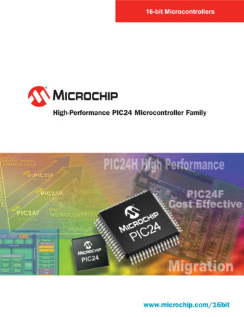
KS8695PXMicrelSystem Level ash/ROM/SRAMSDRAMMemory External I/OWAN I/F10/100 TX/FXAuto MDI-XConsolePortHomePlug8/16/32 BitKS8695PX33MHzPCIIntegrated Multi-PortPCIGateway Solution802.11a/g/b/n4-Port LAN10/100 TX/FXAuto MDI-XFigure 1. KS8695PX PCI Gateway System OptionsSeptember 20055M9999-091605
KS8695PXMicrelPin DescriptionSignal List Alphabetized by NamePin NumberPin NameType(1)U4ADDR0OPin FunctionAddress Bit.T4ADDR1OAddress Bit.R3ADDR10OAddress Bit.P1ADDR11OAddress Bit.P2ADDR12OAddress Bit.N1ADDR13OAddress Bit.N2ADDR14OAddress Bit.N3ADDR15OAddress Bit.N4ADDR16OAddress Bit.M1ADDR17OAddress Bit.M2ADDR18OAddress Bit.M3ADDR19OAddress Bit.U3ADDR2OAddress BitP3ADDR20/BA0OAddress Bit/Bank Address Bit 0 for SDRAM Interface.P4ADDR2/BA1OAddress Bit/Bank Address Bit 1 for SDRAM Interface.T3ADDR3OAddress Bit.U2ADDR4OAddress Bit.U1ADDR5OAddress Bit.T1ADDR6OAddress Bit.T2ADDR7OAddress Bit.R1ADDR8OAddress Bit.R2ADDR9OE3AGNDGndAnalog Signal Ground.H7AGNDGndAnalog Signal Ground.J7AGNDGndAnalog Signal Ground.K7AGNDGndAnalog Signal Ground.L7AGNDGndAnalog Signal Ground.Address Bit.D14CBEN0I/OPCI Commands and Byte Enable 0. Active Low.A11CBEN1I/OPCI Commands and Byte Enable 1. Active Low.B9CBEN2I/OPCI Commands and Byte Enable 2. Active Low.A6CBEN3I/OPCI Commands and Byte Enable 3. Active Low.B10CLKRUNNI/OCardbus Clock Run Request Signal. Active Low.U15DATA0I/OExternal Data Bit.T15DATA1I/OExternal Data Bit.U12DATA10I/OExternal Data Bit.T12DATA11I/OExternal Data Bit.Note:1. Gnd Ground.O Output.I/O Bidirectional.M9999-0916056September 2005
KS8695PXMicrelPin NumberPin NameType(1)R12DATA12I/OExternal Data Bit.P12DATA13I/OExternal Data Bit.U11DATA14I/OExternal Data Bit.Pin FunctionT11DATA15I/OExternal Data Bit.R11DATA16I/OExternal Data Bit.P11DATA17I/OExternal Data Bit.U10DATA18I/OExternal Data Bit.T10DATA19I/OExternal Data Bit.U14DATA2I/OExternal Data Bit.R10DATA20I/OExternal Data Bit.P10DATA21I/OExternal Data Bit.U9DATA22I/OExternal Data Bit.T9DATA23I/OExternal Data Bit.R9DATA24I/OExternal Data Bit.P9DATA25I/OExternal Data Bit.U8DATA26I/OExternal Data Bit.T8DATA27I/OExternal Data Bit.R8DATA28I/OExternal Data Bit.P8DATA29I/OExternal Data Bit.T14DATA3I/OExternal Data Bit.R7DATA30I/OExternal Data Bit.P7DATA31I/OExternal Data Bit.R14DATA4I/OExternal Data Bit.P14DATA5I/OExternal Data Bit.U13DATA6I/OExternal Data Bit.T13DATA7I/OExternal Data Bit.R13DATA8I/OExternal Data Bit.P13DATA9I/OExternal Data Bit.C11DEVSELNI/OPCI Device Select Signal. Active Low.R16ECSN0OExternal I/O Device Chip Select. Active Low.T16ECSN1OExternal I/O Device Chip Select. Active Low.U16ECSN2OExternal I/O Device Chip Select. Active Low.T17EROEN/WRSTPLSO/IROM/SRAM/FLASH and External I/O Output Enable. Active Low. WRSTOPolarity Select. WRSTPLS 0, WRSTO Active High; WRSTPLS 1, ActiveLow.M17ERWEN0/TESTACKOExternal I/O and ROM/SRAM/FLASH Write Byte Enable. Active Low.N17ERWEN1/TESTREQBOExternal I/O and ROM/SRAM/FLASH Write Byte Enable. Active Low.P17ERWEN2/TESTREQAOExternal I/O and ROM/SRAM/FLASH Write Byte Enable. Active Low.Note:1. O Output.I/O Bidirectional.O/I Output in normal mode; input pin during reset.September 20057M9999-091605
KS8695PXMicrelPin NumberPin NameType(1)R17ERWEN3/TICTESTENNOExternal I/O and ROM/SRAM/FLASH Write Byte Enable. Active Low.P16EWAITNIExternal Wait. Active Low.D10FRAMENI/OPCI Bus Frame Signal. Active Low.A1GNDGndSignal Ground.G7GNDGndSignal Ground.G8GNDGndSignal Ground.Pin FunctionG9GNDGndSignal Ground.G10GNDGndSignal Ground.G11GNDGndSignal Ground.H8GNDGndSignal Ground.H9GNDGndSignal Ground.H10GNDGndSignal Ground.H11GNDGndSignal Ground.J8GNDGndSignal Ground.J9GNDGndSignal Ground.J10GNDGndSignal Ground.J11GNDGndSignal Ground.K8GNDGndSignal Ground.K9GNDGndSignal Ground.K10GNDGndSignal Ground.K11GNDGndSignal Ground.L8GNDGndSignal Ground.L9GNDGndSignal Ground.L10GNDGndSignal Ground.L11GNDGndSignal Ground.C4GNT1NOPCI Bus Grant 1. Active Low. Output for Host Bridge Mode and Guest BridgeMode.C3NC—No ConnectC2NC—No ConnectG17GPIO0/EINT0I/OGeneral Purpose I/O Pin. External Interrupt Request Pin.G16GPIO1/EINT1I/OGeneral Purpose I/O Pin. External Interrupt Request Pin.K17GPIO10I/OGeneral Purpose I/O Pin.K16GPIO11I/OGeneral Purpose I/O Pin.K15GPIO12I/OGeneral Purpose I/O Pin.K14GPIO13I/OGeneral Purpose I/O Pin.L17GPIO14I/OGeneral Purpose I/O Pin.Note:1. Gnd Ground.I Input.O Output.I/O Bidirectional.M9999-0916058September 2005
KS8695PXMicrelPin NumberPin NameType(1)Pin FunctionL16GPIO15I/OGeneral Purpose I/O Pin.H17GPIO2/EINT2I/OGeneral Purpose I/O Pin. External Interrupt Request Pin.H16GPIO3/EINT3I/OGeneral Purpose I/O Pin. External Interrupt Request Pin.H15GPIO4/TOUT0I/OGeneral Purpose I/O Pin. Timer 0 Output Pin.H14GPIO5/TOUT1I/OGeneral Purpose I/O Pin. Timer 1 Output Pin.J17GPIO6I/OGeneral Purpose I/O Pin.J16GPIO7I/OGeneral Purpose I/O Pin.J15GPIO8I/OGeneral Purpose I/O Pin.J14GPIO9I/OGeneral Purpose I/O Pin.D7IDSELIA9IRDYNI/OF1ISETISet PHY Transmit Output Current. Connect to Ground with 3.01k3.01kΩ 1% Resistor.B17L1LED0OLAN Port 1 LED Programmable Indicator 0. Active Low.B16L1LED1OLAN Port 1 LED Programmable Indicator 1. Active Low.C17L2LED0OLAN Port 2 LED Programmable Indicator 0. Active Low.C16L2LED1OLAN Port 2 LED Programmable Indicator 1. Active Low.D17L3LED0OLAN Port 3 LED Programmable Indicator 0. Active Low.D16L3LED1OLAN Port 3 LED Programmable Indicator 1. Active Low.E17L4LED0OLAN Port 4 LED Programmable Indicator 0. Active Low.E16L4LED1OLAN Port 4 LED Programmable Indicator 1. Active Low.H4LANRXM1ILAN Port 1 PHY Receive Signal – (differential).J4LANRXM2ILAN Port 2 PHY Receive Signal – (differential).K4LANRXM3ILAN Port 3 PHY Receive Signal – (differential).L4LANRXM4ILAN Port 4 PHY Receive Signal – (differential).H3LANRXP1ILAN Port 1 PHY Receive Signal (differential).J3LANRXP2ILAN Port 2 PHY Receive Signal (differential).K3LANRXP3ILAN Port 3 PHY Receive Signal (differential).L3LANRXP4ILAN Port 4 PHY Receive Signal (differential).H2LANTXM1OLAN Port 1 PHY Transmit Signal – (differential).J2LANTXM2OLAN Port 2 PHY Transmit Signal – (differential).K2LANTXM3OLAN Port 3 PHY Transmit Signal – (differential).L2LANTXM4OLAN Port 4 PHY Transmit Signal – (differential).Initialization Device Select. Active High.PCI Initiator Ready Signal. Active Low.H1LANTXP1OLAN Port 1 PHY Transmit Signal (differential).J1LANTXP2OLAN Port 2 PHY Transmit Signal (differential).K1LANTXP3OLAN Port 3 PHY Transmit Signal (differential).L1LANTXP4OLAN Port 4 PHY Transmit Signal (differential).E4M66ENIPCI 66 MHz Enable.D2MPCIACTNOMiniPCI Active Signal. Active Low.A16PAD0I/OPCI Address and Data 0.Note:1. I Input.O Output.I/O Bidirectional.September 20059M9999-091605
KS8695PXMicrelPin NameType(1)A15PAD1I/OPCI Address and Data 1.B13PAD10I/OPCI Address and Data 10.D13PAD11I/OPCI Address and Data 11.A12PAD12I/OPCI Address and Data 12.Pin NumberPin FunctionC12PAD13I/OPCI Address and Data 13.B12PAD14I/OPCI Address and Data 14.D12PAD15I/OPCI Address and Data 15.C9PAD16I/OPCI Address and Data 16.A8PAD17I/OPCI Address and Data 17.D9PAD18I/OPCI Address and Data 18.B8PAD19I/OPCI Address and Data 19.C15PAD2I/OPCI Address and Data 2.D8PAD20I/OPCI Address and Data 20.A7PAD21I/OPCI Address and Data 21.C7PAD22I/OPCI Address and Data 22.B7PAD23I/OPCI Address and Data 23.C6PAD24I/OPCI Address and Data 24.B6PAD25I/OPCI Address and Data 25.D6PAD26I/OPCI Address and Data 26.A5PAD27I/OPCI Address and Data 27.C5PAD28I/OPCI Address and Data 28.B5PAD29I/OPCI Address and Data 29.B15PAD3I/OPCI Address and Data 3.D5PAD30I/OPCI Address and Data 30.A4PAD31I/OPCI Address and Data 31.D15PAD4I/OPCI Address and Data 4.A14PAD5I/OPCI Address and Data 5.C14PAD6I/OPCI Address and Data 6.B14PAD7I/OPCI Address and Data 7.A13PAD8I/OPCI Address and Data 8.C13PAD9I/OPCI Address and Data 9.C8PARI/OPCI Parity.D3PBMSIPCI Bridge Mode Select. ‘1’ Host Bridge Mode. ‘0’ Guest Bridge Mode.D4PCLKIPCI Bus Clock.A2PCLKOUT0OPCI Clock Output 0.B1PCLKOUT1OPCI Clock Output 1.C1NC—No ConnectD1NC—No ConnectB11PERRNI/OPCI Parity Error Signal. Active Low.A3PRSTNIPCI Reset. Active Low.Notes:1. I Input.O Output.I/O Bidirectional.M9999-09160510September 2005
KS8695PXMicrelPin NumberPin NameType(1)Pin FunctionP15RCSN0OROM/SRAM/FLASH Chip Select. Active Low.R15RCSN1OROM/SRAM/FLASH Chip Select. Active Low.B4REQ1NIPCI Bus Request 1. Active Low. Input for Host Bridge Mode and Guest BridgeMode.B3NC—No ConnectB2NC—No ConnectA17RESETNIKS8695PX Chip Reset. Active Low.T5SDCASNOSDRAM Column Address Strobe. Active Low.P5SDCSN0OSDRAM Chip Select. Active Low Chip Select Pins for SDRAM.R4SDCSN1OSDRAM Chip Select. Active Low Chip Select Pins for SDRAM.T7SDICLKISDRAM Clock In.U7SDOCLKOSystem/SDRAM Clock Out.U6SDQM0OSDRAM Data Input/Output Mask.T6SDQM1OSDRAM Data Input/Output Mask.R6SDQM2OSDRAM Data Input/Output Mask.P6SDQM3OSDRAM Data Input/Output Mask.R5SDRASNOSDRAM Row Address Strobe. Active Low.U5SDWENOSDRAM Write Enable. Active Low.A10SERRNOPCI System Error Signal. Active Low.D11STOPNI/OPCI Stop Signal. Active Low.G14TCKIJTAG Test Clock.F14TDIIJTAG Test Data In.F15TDOOJTAG Test Data Out.M4TEST1IPHY Test Pin (factory reserved test signal).F4TEST2IPHY Test Pin (factory reserved test signal).F17TESTENIChip Test Enable (factory reserved test signal). Must be connected to GND fornormal operationG15TMSIC10TRDYNI/OJTAG Test Mode SelectPCI Target Ready Signal. Active Low.F16TRSTNIJTAG Test Reset. Active Low.M14UCTSN/BISTENIUART Data Set Ready. Active Low. BIST Enable (factory reserved test signal).L15UDCDN/SCANENIUART Data Carrier Detect. Scan Enable (factory reserved test signal).UART Data Set Ready. Active RTSN/CPUCLKSELO/IUART Data Terminal Ready. Active Low. Debug Enable (factory reserved test .signal)UART Ring Indicator/Chip Test Reset (factory reserved test signal).UART Request to Send/CPU Clock Select.Note:1. I Input.O Output.I/O Bidirectional.O/I Output in normal mode; input pin during reset.September 200511M9999-091605
KS8695PXMicrelPin NumberPin NameType(1)N16URXDIN14UTXDOUART Transmit Data.E7VDD1.8PE8VDD1.8P1.8V Digital Core 3.3PPin FunctionUART Receive Data.1.8V Digital Core VDD.1.8V Digital Core VDD.1.8V Digital Core VDD.1.8V Digital Core VDD.1.8V Digital Core VDD.1.8V Digital Core VDD.1.8V Digital Core VDD.1.8V Digital Core VDD.1.8V Digital Core VDD.1.8V Digital Core VDD.1.8V Digital Core VDD.1.8V Digital Core VDD.1.8V Digital Core VDD.1.8V Digital Core VDD.1.8V Digital Core VDD.1.8V Digital Core VDD.1.8V Digital Core VDD.1.8V Digital Core VDD.1.8V Digital Core VDD.3.3V Digital I/O Circuitry VDD.3.3V Digital I/O Circuitry VDD.3.3V Digital I/O Circuitry VDD.3.3V Digital I/O Circuitry VDD.3.3V Digital I/O Circuitry VDD.3.3V Digital I/O Circuitry VDD.3.3V Digital I/O Circuitry VDD.3.3V Digital I/O Circuitry VDD.3.3V Digital I/O Circuitry VDD.3.3V Digital I/O Circuitry VDD.3.3V Digital I/O Circuitry VDD.3.3V Digital I/O Circuitry VDD.3.3V Digital I/O Circuitry VDD.3.3V Digital I/O Circuitry VDD.3.3V digital I/O Circuitry VDD.3.3V Digital I/O Circuitry VDD.3.3V Digital I/O Circuitry VDD.3.3V Digital I/O Circuitry VDD.Notes:1. P Power supply.I Input.O Output.M9999-09160512September 2005
KS8695PXMicrelPin NumberPin IG4WANRXMIWAN PHY Receive Signal – (differential).Pin Function1.8V Analog VDD.1.8V Analog VDD.1.8V Analog VDD.1.8V Analog VDD.1.8V Analog VDD.1.8V Analog VDD.1.8V Analog VDD.1.8V Analog VDD.1.8V Analog VDD.1.8V Analog VDD.3.3V Analog VDD.3.3V Analog VDD.3.3V Analog VDD.3.3V Analog VDD.3.3V Analog VDD.3.3V Analog VDD.3.3V Analog VDD.3.3V Analog VDD.WAN Fiber Signal Detect.G3WANRXPIWAN PHY Receive Signal (differential).G2WANTXMOWAN PHY Transmit Signal – (differential).G1WANTXPOWAN PHY Transmit Signal (differential).E15WLED0/B0SIZE0O/IWAN LED Programmable Indicator 0. Bank 0 Size Bit 0.E14WLED1/B0SIZE1O/IWAN LED Programmable Indicator 1. Bank 0 Size Bit 1.U17WRSTOOWatchdog Timer Reset Output.When EROEN/WRSTPLS 0, Active High.When EROEN/WRSTPLS 1, Active Low.E1XCLK1IExternal Clock In.E2XCLK2IExternal Clock In (negative polarity).Notes:1. P Power supply.I Input.O Output.O/I Output in normal mode; input pin during reset.September 200513M9999-091605
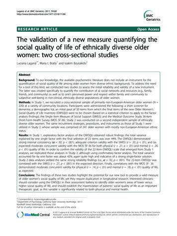
KS8695PXMicrelPin Configuration123AGNDPCLKOUT0 PRSTNBPCLKOUT1 REQ3NREQ2NCPCLKOUT2 5PAD1PAD0RESETNCLKRUNN GNT1NPAD28PAD24PAD22PARPAD16TRDYNDEVSELN PAD13PAD9PAD6PAD2L2LED1L2LED0PCLKOUT3 MPCIACTN XMWANRXPWANRXM O1/EINT1HLANTXP1LANTXM1LANRXP1LANRXM1 2LANRXP2LANRXM2 O8GPIO7GPIO6KLANTXP3LANTXM3LANRXP3LANRXM3 IO12GPIO11GPIO10LLANTXP4LANTXM4LANRXP4LANRXM4 DN/TSTRST BA0ADDR21/BA1SDCSN0SDQM3DATA31 DATA29 DATA25DATA21DATA17DATA13 DATA9DATA5RCSN0EWAITN ERWEN2ADDR9ADDR10SDCSN1SDRASNSDQM2DATA30 DATA28 DATA24DATA20DATA16DATA12 SNSDQM1SDICLKDATA27 DATA23DATA19DATA15DATA11 DR0SDWENSDQM0SDOCLK DATA26 DATA22DATA18DATA14DATA10 11121314151617PCI SignalsLED DriversVDD3.3VDDA3.3UART SignalsMemory InterfaceVDDA1.8AGNDJTAG SignalsGPIOVDD1.8MiscellaneousAnalogGNDFigure 2. KS8695PX Pin Mapping (Top View)M9999-09160514September 2005
KS8695PXMicrelFunctional DescriptionIntroductionMicrel's KS8695PX, a member of the CENTAUR line of integrated processors, is a high-performance router-on-a-chip solution for Ethernet and 802.11 a/g/b based embedded systems. Designed for use in communication's routers, it integrates aPCI to AHB bridge solution for interfacing with 32-bit PCI, miniPCI, and cardbus devices. The KS8695PX combines a proventhird generation 5-port managed switch, an ARM9 RISC processor with MMU, and five physical layer transceivers (PHYs)including their corresponding MAC units with Micrel's XceleRouter technology.The KS8695PX is built around the 16/32-bit ARM9 RISC processor, which is a scalable, high-performance, microprocessordeveloped for highly integrated system-on-a-chip applications. It also offers a configurable 8KB I-cache and 8KB D-cachethat reduces memory access latency for high-performance applications. The simple, elegant, and fully static design of theKS8695PX is especially suitable for cost-effective, power-sensitive applications.The KS8695PX contains five 10/100 PHYs: four are for the local area network (LAN) and one is for the wide area network(WAN). Connected to the PHYs are five corresponding MAC units with an integrated Layer 2 managed switch. The combiningof the switch and the analog PHYs make the KS8695PX an extremely prudent solution for SOHO router applications, savingboth board space and BOM costs. The Layer 2 switch contains a 16Kx32 SRAM on-chip memory for frame buffering. Theembedded frame buffer memory is designed with a 1.4Gbps on-chip memory bus. This allows the KS8695PX to perform fullnon-blocking frame switching and/or routing on the fly for many applicationsFor the media interface, the KS8695PX supports 10BASE-T and 100BASE-TX, as specified by the IEEE 802.3 standard,and 100 BASE-FX on the WAN port and on one LAN portThe KS8695PX supports two modes of operation in the PCI bus environment: host bridge mode and guest bridge mode. In thehost bridge mode, the ARM9 processor acts as the host of the entire system. It configures other PCI devices and coordinatestheir transactions, including initiating transactions between the PCI devices and AHB bus subsystem. An on-chip PCI arbiteris included to determine the PCI bus ownership among PCI master devices. In host bridge mode, all I/O registers, includingthose for the embedded switch, are configured by the ARM9 processor through the on-chip AMBA bus interface.In guest bridge mode, all of the I/O registers are programmed by either the external host CPU on the PCI bus or the localARM9 host processor through the AMBA bus. The KS8695PX functions as a slave on the PCI bus with the on-chip PCI arbiterdisabled. The KS8695PXX can be configured by either the ARM9 CPU or the PCI host CPU. In both cases, the KS8695PXmemory subsystem is accessible from either the PCI host or the ARM9 CPU. Communications between the external hostCPU and the ARM9 is accomplished through message passing or through shared memory.CPU Features 166MHz ARM9 RISC processor coreOn-chip AMBA bus 2.0 interfaces16-bit thumb programming to relax memory requirement8KB I-cache and 8KB D-cacheLittle-endian mode supportedConfigurable memory management unitSupports reduced CPU and system clock speed for power savingsPCI to AHB Bridge Features Support 33MHz, 32-bit data PCI busIntegrated PCI bridge support for interfacing with 32-bit miniPCI or cardbus devicesIndependent AHB and PCI clock speedSupports 125MHz AHB speedSupports PCI revision 2.1 protocolsSupports AHB bus 2.0 interfacesSupports both regular and memory-mapped I/O on the PCI interfaceIntegrated PCI arbiter with power-on option to enable or disableSupport Round Robin arbitration with three external PCI devices and one internal deviceSupports AHB burst transfers up to 16 data wordsConfigurable PCI registers by host CPU ARM9Supports bus mastership from PCI to AHB or AHB to PCI busSwitch Engine 5-Port 10/10
is a single-chip, multi-port PCI "gateway-on-a-chip" with all the key components integrated for a high-performance and low-cost broadband gateway ARM9 High-Performance CPU Core - ARM9 core at 166MHz - 8KB I-cache and 8KB D-cache - Memory management unit (MMU) for Linux and WinCE - 32-bit ARM and 16-bit thumb instruction sets for