Transcription
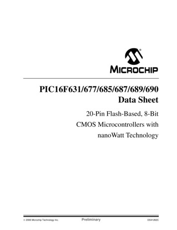
PIC16F631/677/685/687/689/690Data Sheet20-Pin Flash-Based, 8-BitCMOS Microcontrollers withnanoWatt Technology 2006 Microchip Technology Inc.PreliminaryDS41262C
Note the following details of the code protection feature on Microchip devices: Microchip products meet the specification contained in their particular Microchip Data Sheet. Microchip believes that its family of products is one of the most secure families of its kind on the market today, when used in theintended manner and under normal conditions. There are dishonest and possibly illegal methods used to breach the code protection feature. All of these methods, to ourknowledge, require using the Microchip products in a manner outside the operating specifications contained in Microchip’s DataSheets. Most likely, the person doing so is engaged in theft of intellectual property. Microchip is willing to work with the customer who is concerned about the integrity of their code. Neither Microchip nor any other semiconductor manufacturer can guarantee the security of their code. Code protection does notmean that we are guaranteeing the product as “unbreakable.”Code protection is constantly evolving. We at Microchip are committed to continuously improving the code protection features of ourproducts. Attempts to break Microchip’s code protection feature may be a violation of the Digital Millennium Copyright Act. If such actsallow unauthorized access to your software or other copyrighted work, you may have a right to sue for relief under that Act.Information contained in this publication regarding deviceapplications and the like is provided only for your convenienceand may be superseded by updates. It is your responsibility toensure that your application meets with your specifications.MICROCHIP MAKES NO REPRESENTATIONS ORWARRANTIES OF ANY KIND WHETHER EXPRESS ORIMPLIED, WRITTEN OR ORAL, STATUTORY OROTHERWISE, RELATED TO THE INFORMATION,INCLUDING BUT NOT LIMITED TO ITS CONDITION,QUALITY, PERFORMANCE, MERCHANTABILITY ORFITNESS FOR PURPOSE. Microchip disclaims all liabilityarising from this information and its use. Use of Microchipdevices in life support and/or safety applications is entirely atthe buyer’s risk, and the buyer agrees to defend, indemnify andhold harmless Microchip from any and all damages, claims,suits, or expenses resulting from such use. No licenses areconveyed, implicitly or otherwise, under any Microchipintellectual property rights.TrademarksThe Microchip name and logo, the Microchip logo, Accuron,dsPIC, KEELOQ, microID, MPLAB, PIC, PICmicro, PICSTART,PRO MATE, PowerSmart, rfPIC and SmartShunt areregistered trademarks of Microchip Technology Incorporatedin the U.S.A. and other countries.AmpLab, FilterLab, Migratable Memory, MXDEV, MXLAB,SEEVAL, SmartSensor and The Embedded Control SolutionsCompany are registered trademarks of Microchip TechnologyIncorporated in the U.S.A.Analog-for-the-Digital Age, Application Maestro, CodeGuard,dsPICDEM, dsPICDEM.net, dsPICworks, ECAN,ECONOMONITOR, FanSense, FlexROM, fuzzyLAB,In-Circuit Serial Programming, ICSP, ICEPIC, Linear ActiveThermistor, Mindi, MiWi, MPASM, MPLIB, MPLINK, PICkit,PICDEM, PICDEM.net, PICLAB, PICtail, PowerCal,PowerInfo, PowerMate, PowerTool, REAL ICE, rfLAB,rfPICDEM, Select Mode, Smart Serial, SmartTel, TotalEndurance, UNI/O, WiperLock and ZENA are trademarks ofMicrochip Technology Incorporated in the U.S.A. and othercountries.SQTP is a service mark of Microchip Technology Incorporatedin the U.S.A.All other trademarks mentioned herein are property of theirrespective companies. 2006, Microchip Technology Incorporated, Printed in theU.S.A., All Rights Reserved.Printed on recycled paper.Microchip received ISO/TS-16949:2002 certification for its worldwideheadquarters, design and wafer fabrication facilities in Chandler andTempe, Arizona, Gresham, Oregon and Mountain View, California. TheCompany’s quality system processes and procedures are for itsPICmicro 8-bit MCUs, KEELOQ code hopping devices, SerialEEPROMs, microperipherals, nonvolatile memory and analogproducts. In addition, Microchip’s quality system for the design andmanufacture of development systems is ISO 9001:2000 certified.DS41262C-page iiPreliminary 2006 Microchip Technology Inc.
PIC16F631/677/685/687/689/69020-Pin Flash-Based, 8-Bit CMOS Microcontrollers withnanoWatt TechnologyHigh-Performance RISC CPU:Low-Power Features: Only 35 instructions to learn:- All single-cycle instructions except branches Operating speed:- DC – 20 MHz oscillator/clock input- DC – 200 ns instruction cycle Interrupt capability 8-level deep hardware stack Direct, Indirect and Relative Addressing modes Standby Current:- 50 nA @ 2.0V, typical Operating Current:- 11 μA @ 32 kHz, 2.0V, typical- 220 μA @ 4 MHz, 2.0V, typical Watchdog Timer Current:- 1 μA @ 2.0V, typicalPeripheral Features:Special Microcontroller Features: Precision Internal Oscillator:- Factory calibrated to 1%- Software selectable frequency range of8 MHz to 32 kHz- Software tunable- Two-Speed Start-up mode- Crystal fail detect for critical applications- Clock mode switching during operation forpower savings Power-Saving Sleep mode Wide operating voltage range (2.0V-5.5V) Industrial and Extended Temperature range Power-on Reset (POR) Power-up Timer (PWRTE) and Oscillator Start-upTimer (OST) Brown-out Reset (BOR) with software controloption Enhanced low-current Watchdog Timer (WDT)with on-chip oscillator (software selectablenominal 268 seconds with full prescaler) withsoftware enable Multiplexed Master Clear/Input pin Programmable code protection High Endurance Flash/EEPROM cell:- 100,000 write Flash endurance- 1,000,000 write EEPROM endurance- Flash/Data EEPROM retention: 40 years Enhanced USART module:- Supports RS-485, RS-232 and LIN 2.0- Auto-Baud Detect- Auto-wake-up on Start bit 2006 Microchip Technology Inc. 17 I/O pins and 1 input only pin:- High current source/sink for direct LED drive- Interrupt-on-Change pin- Individually programmable weak pull-ups- Ultra Low-Power Wake-up (ULPWU) Analog Comparator module with:- Two analog comparators- Programmable on-chip voltage reference(CVREF) module (% of VDD)- Comparator inputs and outputs externallyaccessible- SR Latch mode- Timer 1 Gate Sync Latch- Fixed 0.6V VREF A/D Converter:- 10-bit resolution and 12 channels Timer0: 8-bit timer/counter with 8-bitprogrammable prescaler Enhanced Timer1:- 16-bit timer/counter with prescaler- External Timer1 Gate (count enable)- Option to use OSC1 and OSC2 in LP modeas Timer1 oscillator if INTOSC modeselected Timer2: 8-bit timer/counter with 8-bit periodregister, prescaler and postscaler Enhanced Capture, Compare, PWM module:- 16-bit Capture, max resolution 12.5 ns- Compare, max resolution 200 ns- 10-bit PWM with 1, 2 or 4 output channels,programmable “dead time”, max frequency20 kHz- PWM output steering control Synchronous Serial Port (SSP):- SPI mode (Master and Slave) I2C (Master/Slave modes):- I2C address mask In-Circuit Serial ProgrammingTM (ICSPTM) via twopinsPreliminaryDS41262C-page 1
PIC16F631/677/685/687/689/690ProgramMemoryData MemoryFlash(words)SRAM EEPROM(bytes) 5612825625612825625625625625610-bit imers8/16-bitSSP ECCP oYesNoNoNoYesYesYesPIC16F631 Pin A3/MCLR/VPPRC5RC4/C2OUTRC3/C12IN3RC6RC7RB7TABLE 1:12345678910PIC16F63120-pin PDIP, SOIC, SSOP20191817161514131211VSSRA0/C1IN UTRC0/C2IN RC1/C12IN1RC2/C12IN2RB4RB5RB6PIC16F631 PIN upBasicRA019AN0/ULPWUC1IN 2IN �VDD—20—————VSSNote 1:Pull-up enabled only with external MCLR configuration.DS41262C-page 2Preliminary 2006 Microchip Technology Inc.
PIC16F631/677/685/687/689/690PIC16F677 Pin RC7/AN9/SDORB7TABLE 2:12345678910PIC16F67720-pin PDIP, SOIC, SSOP20191817161514131211VSSRA0/AN0/C1IN T0CKI/INT/C1OUTRC0/AN4/C2IN 11RB6/SCK/SCLPIC16F677 PIN ll-upBasicRA019AN0/ULPWUC1IN L/SCKIOCY—RB710————IOCY—RC016AN4C2IN —VSSNote 1:Pull-up activated only with external MCLR configuration. 2006 Microchip Technology Inc.PreliminaryDS41262C-page 3
PIC16F631/677/685/687/689/690PIC16F685 Pin 2IN3-/P1CRC6/AN8RC7/AN9RB7TABLE 3:12345678910PIC16F68520-pin PDIP, SOIC, SSOP20191817161514131211VSSRA0/AN0/C1IN T0CKI/INT/C1OUTRC0/AN4/C2IN B6PIC16F685 PIN ull-upBasicRA019AN0/ULPWUC1IN Y————IOCY—MCLR/VPPRC016AN4C2IN ———VSSNote 1:Pull-up activated only with external MCLR configuration.DS41262C-page 4Preliminary 2006 Microchip Technology Inc.
PIC16F631/677/685/687/689/690PIC16F687/689 Pin SRC7/AN9/SDORB7/TX/CKTABLE 4:12345678910PIC16F687/68920-pin PDIP, SOIC, SSOP20191817161514131211VSSRA0/AN0/C1IN T0CKI/INT/C1OUTRC0/AN4/C2IN 11/RX/DTRB6/SCK/SCLPIC16F687/689 PIN AN0/ULPWUC1IN CKI—RA34———RA43AN3—Interrupt RC016AN4C2IN �—VDD—20———————VSSNote 1: Pull-up activated only with external MCLR configuration. 2006 Microchip Technology Inc.PreliminaryDS41262C-page 5
PIC16F631/677/685/687/689/690PIC16F690 Pin Diagram (PDIP, SOIC, N3-/P1CRC6/AN8/SSRC7/AN9/SDORB7/TX/CKTABLE 5:I/O12345678910PIC16F69020-pin PDIP, SOIC, SSOP20191817161514131211VSSRA0/AN0/C1IN T0CKI/INT/C1OUTRC0/AN4/C2IN B5/AN11/RX/DTRB6/SCK/SCLPIC16F690 PIN SUMMARYPinAnalogComparators LPWUC1IN 16AN4C2IN —————VSSNote 1: Pull-up activated only with external MCLR configuration.DS41262C-page 6Preliminary 2006 Microchip Technology Inc.
PIC16F631/677/685/687/689/690PIC16F690 Pin Diagram /CLKOUTRA5/T1CKI/OSC1/CLKINVDDVSSRA0/AN0/C1IN /ICSPDAT/ULPWU201918171620-pin N CK(3)6RC7/AN9/SDO(2)Note SCL(2)(1)CCP1/P1A, P1B, P1C and P1D are available on PIC16F685/PIC16F690 only.2:SS, SDO, SDI/SDA and SCL/SCK are available on PIC16F677/PIC16F687/PIC16F689/PIC16F690 only.3:RX/DT and TX/CK are available on PIC16F687/PIC16F689/PIC16F690 only. 2006 Microchip Technology Inc.PreliminaryDS41262C-page 7
PIC16F631/677/685/687/689/690Table of Contents1.0 Device Overview . 92.0 Memory Organization . 253.0 Oscillator Module (With Fail-Safe Clock Monitor). 474.0 I/O Ports . 595.0 Timer0 Module . 816.0 Timer1 Module with Gate Control. 847.0 Timer2 Module . 918.0 Comparator Module. 939.0 Analog-to-Digital Converter (ADC) Module . 10710.0 Data EEPROM and Flash Program Memory Control . 11911.0 Enhanced Capture/Compare/PWM Module . 12712.0 Enhanced Universal Synchronous Asynchronous Receiver Transmitter (EUSART) . 14913.0 SSP Module Overview . 17514.0 Special Features of the CPU . 19315.0 Instruction Set Summary . 21316.0 Development Support. 22317.0 Electrical Specifications. 22718.0 DC and AC Characteristics Graphs and Tables . 25519.0 Packaging Information. 275Appendix A: Data Sheet Revision History. 281Appendix B: Migrating from other PICmicro Devices . 281TO OUR VALUED CUSTOMERSIt is our intention to provide our valued customers with the best documentation possible to ensure successful use of your Microchipproducts. To this end, we will continue to improve our publications to better suit your needs. Our publications will be refined andenhanced as new volumes and updates are introduced.If you have any questions or comments regarding this publication, please contact the Marketing Communications Department via Email at docerrors@microchip.com or fax the Reader Response Form in the back of this data sheet to (480) 792-4150. We welcome your feedback.Most Current Data SheetTo obtain the most up-to-date version of this data sheet, please register at our Worldwide Web site at:http://www.microchip.comYou can determine the version of a data sheet by examining its literature number found on the bottom outside corner of any page.The last character of the literature number is the version number, (e.g., DS30000A is version A of document DS30000).ErrataAn errata sheet, describing minor operational differences from the data sheet and recommended workarounds, may exist for currentdevices. As device/documentation issues become known to us, we will publish an errata sheet. The errata will specify the revision ofsilicon and revision of document to which it applies.To determine if an errata sheet exists for a particular device, please check with one of the following: Microchip’s Worldwide Web site; http://www.microchip.com Your local Microchip sales office (see last page)When contacting a sales office, please specify which device, revision of silicon and data sheet (include literature number) you areusing.Customer Notification SystemRegister on our web site at www.microchip.com to receive the most current information on all of our products.DS41262C-page 8Preliminary 2006 Microchip Technology Inc.
PIC16F631/677/685/687/689/6901.0DEVICE OVERVIEWBlock Diagrams and pinout descriptions of the devicesare as follows:The PIC16F631/677/685/687/689/690 devices arecovered by this data sheet. They are available in 20-pinPDIP, SOIC, TSSOP and QFN packages.FIGURE 1-1: PIC16F631 (Figure 1-1, Table 1-1)PIC16F677 (Figure 1-2, Table 1-2)PIC16F685 (Figure 1-3, Table 1-3)PIC16F687/PIC16F689 (Figure 1-4, Table 1-4)PIC16F690 (Figure 1-5, Table 1-5)PIC16F631 BLOCK DIAGRAMINTConfiguration138Data BusPORTAProgram CounterRA0RA1RA2RA3RA4RA5Flash1K x 14ProgramRAM64 bytesFileRegisters8-Level Stack (13-bit)MemoryProgram 14BusRAM Addr9PORTBAddr MUXInstruction Reg7Direct Addr8RB4RB5RB6RB7IndirectAddrFSR RegSTATUS Reg8PORTC3Power-upTimerInstructionDecode andControlOscillatorStart-up ationRC0RC1RC2RC3RC4RC5RC6RC7MUX8WatchdogTimerW RegBrown-outResetInternalOscillatorBlockMCLR VDDULPWUUltra Low-PowerWake-upT0CKIVSST1GT1CKIC1IN- C1IN C1OUT C2IN- C2IN C2OUTEEDAT128 BytesDataEEPROMTimer0Timer1EEADR2Analog Comparatorsand Reference8 2006 Microchip Technology Inc.PreliminaryDS41262C-page 9
PIC16F631/677/685/687/689/690FIGURE 1-2:PIC16F677 BLOCK DIAGRAMINTConfiguration138Data BusPORTAProgram CounterFlashRA0RA1RA2RA3RA4RA52K x 14ProgramRAM128 bytesFileRegisters8-Level Stack (13-bit)MemoryProgram 14BusRAM Addr9PORTBAddr MUXInstruction Reg7Direct Addr8IndirectAddrRB4RB5RB6RB7FSR RegSTATUS Reg8PORTC3Power-upTimerInstructionDecode andControlOscillatorStart-up ationRC0RC1RC2RC3RC4RC5RC6RC7MUX8WatchdogTimerW RegBrown-outResetInternalOscillatorBlockMCLR VDDULPWUT0CKIUltra Low-PowerWake-upTimer0VSST1GSDI/ SCK/SDO SDA SCL SST1CKISynchronousSerial PortTimer1AN8 AN9 AN10 AN11EEDATAnalog-To-Digital Converter2Analog Comparatorsand Reference8256 BytesDataEEPROMEEADRVREF AN0 AN1 AN2 AN3 AN4 AN5 AN6 AN7 C1IN- C1IN C1OUT C2IN- C2IN C2OUTDS41262C-page 10Preliminary 2006 Microchip Technology Inc.
PIC16F631/677/685/687/689/690FIGURE 1-3:PIC16F685 BLOCK DIAGRAMINTConfiguration138Data BusPORTAProgram CounterFlashRA0RA1RA2RA3RA4RA54K x 14ProgramRAM256 bytesFileRegisters8-Level Stack (13-bit)MemoryProgram 14BusRAM Addr9PORTBAddr MUXInstruction Reg7Direct Addr8IndirectAddrRB4RB5RB6RB7FSR RegSTATUS Reg8PORTC3Power-upTimerInstructionDecode andControlOscillatorStart-up ationRC0RC1RC2RC3RC4RC5RC6RC7MUX8WatchdogTimerW RegBrown-outResetInternalOscillatorBlockMCLR VDDULPWUT0CKIUltra Low-PowerWake-upTimer0VSST1GCCP1/P1A P1B P1C P1DT1CKITimer1Timer2ECCP AN8 AN9 AN10 AN11EEDATAnalog-To-Digital Converter2Analog Comparatorsand Reference8256 BytesDataEEPROMEEADRVREF AN0 AN1 AN2 AN3 AN4 AN5 AN6 AN7 C1IN- C1IN C1OUT C2IN- C2IN C2OUT 2006 Microchip Technology Inc.PreliminaryDS41262C-page 11
PIC16F631/677/685/687/689/690FIGURE 1-4:PIC16F687/PIC16F689 BLOCK DIAGRAMINTConfiguration138Data BusPORTAProgram CounterFlashRA0RA1RA2RA3RA4RA52K(1)/4K x 14ProgramRAM128(1)/256 bytesFileRegisters8-Level Stack (13-bit)MemoryProgram 14BusRAM Addr9PORTBAddr MUXInstruction RegIndirectAddr7Direct Addr8RB4RB5RB6RB7FSR RegSTATUS Reg8PORTC3Power-upTimerInstructionDecode andControlOscillatorStart-up /CLKORC0RC1RC2RC3RC4RC5RC6RC7MUX8WatchdogTimerW RegBrown-outResetInternalOscillatorBlockMCLR VDDULPWUT0CKIUltra Low-PowerWake-upTimer0VSST1GT1CKITimer1TX/CKSDI/ SCK/SDO SDA SCL SSRX/DTSynchronousSerial PortEUSARTAN8 AN9 AN10 AN11EEDATAnalog-To-Digital Converter2Analog Comparatorsand Reference8256 BytesDataEEPROMEEADRVREF AN0 AN1 AN2 AN3 AN4 AN5 AN6 AN7 C1IN- C1IN C1OUT C2IN- C2IN C2OUTNote1:DS41262C-page 12PIC16F687 only.Preliminary 2006 Microchip Technology Inc.
PIC16F631/677/685/687/689/690FIGURE 1-5:PIC16F690 BLOCK DIAGRAMINTConfiguration138Data BusPORTAProgram CounterFlashRA0RA1RA2RA3RA4RA54k x 14ProgramRAM256 bytesFileRegisters8-Level Stack (13-bit)MemoryProgram 14BusRAM Addr9PORTBAddr MUXInstruction RegDirect Addr78IndirectAddrRB4RB5RB6RB7FSR RegSTATUS Reg8PORTC3Power-upTimerInstructionDecode andControlOscillatorStart-up onRC0RC1RC2RC3RC4RC5RC6RC7MUXALU8WatchdogTimerW RegBrown-outResetInternalOscillatorBlockMCLR VDDULPWUT0CKIUltra Low-PowerWake-upTimer0T1GVSSTX/CK RX/DTT1CKITimer1Timer2CCP1/P1AEUSARTP1B P1C P1DECCP SDI/ SCK/SDO SDA SCL SSSynchronousSerial PortAN8 AN9 AN10 AN11EEDATAnalog-To-Digital Converter2Analog Comparatorsand Reference8256 BytesDataEEPROMEEADRVREF AN0 AN1 AN2 AN3 AN4 AN5 AN6 AN7 C1IN- C1IN C1OUT C2IN- C2IN C2OUT 2006 Microchip Technology Inc.PreliminaryDS41262C-page 13
PIC16F631/677/685/687/689/690TABLE 1-1:PINOUT DESCRIPTION – PIC16F631NameRA0/C1IN KINFunctionInputTypeRA0TTLC1IN ANICSPDATSTULPWUANRA1TTLOutputTypeDescriptionCMOS General purpose I/O. Individually controlled interrupt-on-change.Individually enabled pull-up.—Comparator C1 non-inverting input.CMOS ICSP Data I/O.—Ultra Low-Power Wake-up input.CMOS General purpose I/O. Individually controlled interrupt-on-change.Individually enabled pull-up.C12IN0-AN—Comparator C1 or C2 inverting input.ICSPCLKST—ICSP clock.RA2STT0CKIST—Timer0 clock input.INTST—External interrupt pin.C1OUT—RA3TTL—General purpose input. Individually controlled interrupt-onchange.MCLRST—Master Clear with internal pull-up.—Programming voltage.CMOS General purpose I/O. Individually controlled interrupt-on-change.Individually enabled pull-up.CMOS Comparator C1 output.VPPHVRA4TTLT1GST—Timer1 gate CMOS General purpose I/O. Individually controlled interrupt-on-change.Individually enabled pull-up.CMOS FOSC/4 output.CMOS General purpose I/O. Individually controlled interrupt-on-change.Individually enabled pull-up.T1CKIST—Timer1 clock input.OSC1XTAL—Crystal/Resonator.—External clock input/RC oscillator connection.CLKINSTRB4RB4TTLCMOS General purpose I/O. Individually controlled interrupt-on-change.Individually enabled pull-up.RB5RB5TTLCMOS General purpose I/O. Individually controlled interrupt-on-change.Individually enabled pull-up.RB6RB6TTLCMOS General purpose I/O. Individually controlled interrupt-on-change.Individually enabled pull-up.RB7RB7TTLCMOS General purpose I/O. Individually controlled interrupt-on-change.Individually enabled pull-up.CMOS General purpose I/O.RC0/C2IN C0STC2IN omparator C2 non-inverting input.—Comparator C1 or C2 inverting input.CMOS General purpose I/O.—Comparator C1 or C2 inverting input.CMOS General purpose I/O.—Comparator C1 or C2 inverting input.CMOS General purpose I/O.C2OUT—CMOS Comparator C2 output.RC5STCMOS General purpose I/O.AN Analog input or outputTTL TTL compatible inputHV High VoltageDS41262C-page 14—CMOS General purpose I/O.CMOS CMOS compatible input or outputST Schmitt Trigger input with CMOS levelsXTAL CrystalPreliminary 2006 Microchip Technology Inc.
PIC16F631/677/685/687/689/690TABLE 1-1:PINOUT DESCRIPTION – PIC16F631 (CONTINUED)FunctionInputTypeRC6RC6STCMOS General purpose I/O.RC7RC7STCMOS General purpose I/O.VSSVSSPower—Ground reference.VDDVDDPower—Positive supply.NameLegend:AN Analog input or outputTTL TTL compatible inputHV High Voltage 2006 Microchip Technology Inc.OutputTypeDescriptionCMOS CMOS compatible input or outputST Schmitt Trigger input with CMOS levelsXTAL CrystalPreliminaryDS41262C-page 15
PIC16F631/677/685/687/689/690TABLE 1-2:PINOUT DESCRIPTION – PIC16F677NameRA0/AN0/C1IN K/SCLLegend:FunctionInputTypeRA0TTLDescriptionCMOS General purpose I/O. Individually controlled interrupt-on-change.Individually enabled pull-up.AN0AN—A/D Channel 0 input.C1IN AN—Comparator C1 non-inverting input.ICSPDATSTULPWUANRA1TTLCMOS ICSP Data I/O.—Ultra Low-Power Wake-up input.CMOS General purpose I/O. Individually controlled interrupt-on-change.Individually enabled pull-up.AN1AN—A/D Channel 1 input.C12IN0-AN—Comparator C1 or C2 inverting input.VREFAN—External Voltage Reference for A/D.ICSPCLKST—ICSP clock.RA2STAN2AN—A/D Channel 2 input.T0CKIST—Timer0 clock input.INTST—External interrupt pin.C1OUT—RA3TTLCMOS General purpose I/O. Individually controlled interrupt-on-change.Individually enabled pull-up.CMOS Comparator C1 output.—General purpose input. Individually controlled interrupt-onchange.MCLRST—Master Clear with internal pull-up.VPPHV—Programming voltage.RA4TTLAN3ANT1GST—Timer1 gate CMOS General purpose I/O. Individually controlled interrupt-on-change.Individually enabled pull-up.—A/D Channel 3 input.CMOS FOSC/4 output.CMOS General purpose I/O. Individually controlled interrupt-on-change.Individually enabled pull-up.T1CKIST—Timer1 clock input.OSC1XTAL—Crystal/Resonator.—External clock input/RC oscillator connection.CLKINSTRB4TTLAN10AN—A/D Channel 10 input.SDIST—SPI data input.SDASTODI2C data input/output.RB5TTLCMOS General purpose I/O. Individually controlled interrupt-on-change.Individually enabled pull-up.CMOS General purpose I/O. Individually controlled interrupt-on-change.Individually enabled pull-up.AN11ANRB6TTLCMOS General purpose I/O. Individually controlled interrupt-on-change.Individually enabled pull-up.SCKSTCMOS SPI clock.SCLSTAN Analog input or outputTTL TTL compatible inputHV High VoltageDS41262C-page 16OutputType—ODA/D Channel 11 input.I2C clock.CMOS CMOS compatible input or outputST Schmitt Trigger input with CMOS levelsXTAL CrystalPreliminary 2006 Microchip Technology Inc.
PIC16F631/677/685/687/689/690TABLE 1-2:PINOUT DESCRIPTION – PIC16F677 (CONTINUED)FunctionInputTypeRB7RB7TTLCMOS General purpose I/O. Individually controlled interrupt-on-change.Individually enabled pull-up.RC0/AN4/C2IN RC0STCMOS General purpose I/O.AN4ANC2IN 12IN3-RC4/C2OUTOutputTypeDescription—A/D Channel 4 input.—Comparator C2 non-inverting input.CMOS General purpose I/O.AN5AN—A/D Channel 5 input.C12IN1-AN—Comparator C1 or C2 inverting input.RC2STAN6ANCMOS General purpose I/O.—A/D Channel 6 input.C12IN2-AN—Comparator C1 or C2 inverting input.RC3STCMOS General purpose I/O.AN7AN—A/D Channel 7 input.C12IN3-AN—Comparator C1 or C2 inverting input.RC4STCMOS General purpose I/O.C2OUT—CMOS Comparator C2 output.RC5RC5STCMOS General purpose I/O.RC6/AN8/SSRC6STCMOS General purpose I/O.AN8AN—A/D Channel 8 input.SSST—Slave Select ower—Ground reference.VDDPower—Positive supply.AN Analog input or outputTTL TTL compatible inputHV High Voltage 2006 Microchip Technology Inc.CMOS General purpose I/O.—A/D Channel 9 input.CMOS SPI data output.CMOS CMOS compatible input or outputST Schmitt Trigger input with CMOS levelsXTAL CrystalPreliminaryDS41262C-page 17
PIC16F631/677/685/687/689/690T
2006 Microchip Technology Inc. Preliminary DS41262C-page 5 PIC16F631/677/685/687/689/690 PIC16F687/689 Pin Diagram TABLE 4: PIC16F687/689 PIN SUMMARY 20-pin PDIP .