Transcription
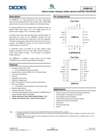
ZXBM1021SINGLE PHASE VARIABLE SPEED MOTOR CONTROL PRE-DRIVERPin AssignmentsThe ZXBM1021 is a high performance, low noise, single-phase,VCCFor system flexibility the motor speed can be controlled by either anH H-speed control and current control suitable for fan and blower motors.Ph2Hi(Top View)Direct Current Brushless (BLDC) motor pre-driver with variable PWMV OPDescriptionexternal PWM control signal or by a DC voltage signal from anexternal control voltage or from a Thermistor network.HBIASPh1LoTo prevent motor inrush current the device has a soft start feature. ToThRefPh2Lohelp protect the motor coil, the ZXBM1021 provides rotor lockPWMSPDprotection which shuts down the output drive if rotor lock is detected.ZXBM1021Ph1HiSPDSetThRefThe device automatically re-starts with soft-start when the rotor lock isCSPDremoved. The ZXBM1021 monitors the motor current to provide aSenseFrequency Generator (FG) pin which allows external interface tomonitor motor rotation or speed.SetThFGGNDA Tachometer output is provided by the open collector outputCLCKSMINprogrammable over current limit.U-QFN4040-20The FG output is the magneticchange frequency.(Top View)The ZXBM1021 is available in space saving and low profileU-QFN4040-20 and industry standard QSOP-20 packages.VccFeatures Operating voltage: 6.8V to 18V Can be extended with external regulator120V OPH Ph2HiH-Ph1LoHBIASPh2LoThRefPh1HiZXBM1021SetThRef Speed control via external PWM, DC or Thermistor signals Low noise, high efficiencySPD Soft startCSPDSetTh Integrated current controlSMINFG Reference voltage outputCLCK Built-in Hall amplifier for direct connection of Hall element Rotor Lock Protection PWMSPDSense1110GNDQSOP-20Lock detection, output shutdown and automatic re-start Minimum speed setting Frequency generator (FG) outputApplications Thermally enhanced space saving low profile U-QFN4040-20 and Personal, servers and mainframe computers cooling fansindustry standard QSOP-20 packages Instrumentation and equipment cooling fansTotally Lead-Free & Fully RoHS Compliant (Notes 1 & 2) Home appliance fans and blowersHalogen and Antimony Free. “Green” Device (Note 3) Central heating blowers and extraction systems Industrial fans, blower and extractors Hand dryers Hand-held power tools PumpsNotes:1. No purposely added lead. Fully EU Directive 2002/95/EC (RoHS) & 2011/65/EU (RoHS 2) compliant.2. See http://www.diodes.com/quality/lead free.html for more information about Diodes Incorporated’s definitions of Halogen- and Antimony-free, "Green"and Lead-free.3. Halogen- and Antimony-free "Green” products are defined as those which contain 900ppm bromine, 900ppm chlorine ( 1500ppm total Br Cl) and 1000ppm antimony compounds.ZXBM1021Document number: DS36322 Rev. 2 - 21 of 25www.diodes.comApril 2014 Diodes Incorporated
ZXBM1021Typical Applications Circuit (Note �F22100ΩSPDR7Sense hRefSMINC2R61kΩH PWMSPDPWM control3V l Applications Circuit for PWM Controlusing the ZXBM1021 and ZXMC MOSFET 1/2 Bridge &82.2µF22100ΩSetThRefR7Sense 3Q1-4ZXMC3A17DN85&6470ΩR2SPDCLCKR1016kΩR61kΩH PWMSPDDC control3V OPC30.47µFFG0VTypical Applications Circuit for DC Controlusing the ZXBM1021 and ZXMC MOSFET 1/2 Bridge DriversNote:4. FG pull-up resistor is not shown in the typical application circuit. Generally, the FG pull-up resistor is located at the system host end rather than thefan motor PCB.ZXBM1021Document number: DS36322 Rev. 2 - 22 of 25www.diodes.comApril 2014 Diodes Incorporated
ZXBM1021Pin DescriptionsPackage types: U-QFN4040-20 and QSOP-20Pin NumberU-QFN4040-20 QSOP-20PinNameDescriptionHall Bias Supply Voltage Output Pin. Output voltage is 1.75V typical to supply the external unbuffered (‘naked’) Hall element. A resistance can be added in series with Hall element if lower biasvoltage is efPh1HiPh2Hi1518Ph2Lo1619Ph1Lo1720V OP181VCCPower Supply Pin192023H H-Hall Device Positive Input Pin. When H is higher in relation to H-, Ph2 is active.Hall Device Negative Input PinZXBM1021Document number: DS36322 Rev. 2 - 25V Reference Voltage Output Pin. This voltage is used to supply the external networks.Speed Control PWM Signal Input Pin. PWM signal should be between 0% to 100% duty ratio.DC Voltage Speed Control Input Pin. The control signal voltage should be between 3V for 0%(stop) to 1V for 100% (full speed) speed control. In DC voltage mode, connect a capacitor betweenSPD and ground.Output Pin of the PWM Speed Control Input Signal Integrator. In PWM speed control mode,connect a 0.1 F capacitor from CSPD pin to ground and connect CSPD pin to SPD pin. In DCvoltage speed control mode, leave this pin unconnected.Minimum Speed Setting Pin. Voltage between 3V to 1V on this pin sets the minimum speed themotor is run at between 0% to full speed. The lowest minimum speed achieved depends on themotor coil design.Rotor Lock Detect, Auto Restart Timing and Soft-Start Timing Control Pin. Typically a 470nFcapacitor is connected to this pin to set the soft-start (to full speed), lock detect and restart timings.Supply Return Ground PinFrequency Generator Output to Provide a Tachometer Signal. This is a buffered output from theHall amplifier.Current Sense Threshold Setting Pin. Used to set the threshold voltage that represents themaximum current to be taken by the motor. The current sense voltage at Sense pin is compared tothe SetTh voltage.Current Sense Pin. Input for the signal from a sense resistor in the ground return of the H-bridgecircuit to represent the current taken by the motor.A variable voltage source used to set the voltage on the SetTh pin.Phase 1 High-Side External Power Switch Drive Output Pin. This is a 50mA open-collector output.Phase 2 High-Side External Power Switch Drive Output Pin. This is a 50mA open-collector output.Phase-2 Low-Side External Power Switch Drive Output Pin. Darlington emitter follower output withactive pull down to give source/sink current of 100mA/100mA.Phase-1 Low-Side External Power Switch Drive Output Pin. Darlington emitter follower output withactive pull down to give source/sink current of 100mA/100mA.Phase Low Output Supply Pin. Only the low side output drives for Ph1Lo and Ph2Lo are suppliedby the V OP pin. For external MOSFET power devices, a resistor from VCC pin to V OP slowsdown the turn-on speed of the low-side MOSFET S and therefore helps prevent shoot-throughduring turn-on of low-side switches. For external Bipolar power devices, a resistor between theVCC pin and V OP controls the current into the transistor base.3 of 25www.diodes.comApril 2014 Diodes Incorporated
ZXBM1021Functional Block Diagram (Note 5)D2VccVccV OPThRefPWMSPDPWMSPDPWM speed controlPh1 HiVrefPWMIntegratorPh2 HiPhaseDriveCSPDSPDVSPDVoltage Speed ControlPWM OscVccPh1 LoSMINCLCKPhaseDrive &ControlSet MinSpeedVccPh2 iasH HallH-HallAmpCurrentMonitorSetThRDSpeed &LockDetectVccFGGndNote:5. The ZXBM1021 has an open-collector FG. Typically a pull-up resistor of 10kΩ is recommended from FG pin to the supply voltage.ZXBM1021Document number: DS36322 Rev. 2 - 24 of 25www.diodes.comApril 2014 Diodes Incorporated
ZXBM1021Absolute Maximum Ratings (Note 6) @TA 25 C, unless otherwise specified.)SymbolCharacteristicsValuesVCCMAXSupply Voltage (Note 7)ICCMAXIC Input CurrentPDMAXPower Dissipation(See thermal de-rating curve on ‘Thermal Performance’ section)Unit-0.6 to 20V200mA820820mWmW-55 to 150 CU-QFN4040-20QSOP-20TSTStorage Temperature RangeTJMaximum Junction Temperature150 CHuman Body Model (HBM) ESD CapabilityMachine Model (MM) ESD Protection2300kVVESD HBMESD MMNotes:6. Stresses greater than the 'Absolute Maximum Ratings' specified above may cause permanent damage to the device. These are stress ratings only;functional operation of the device at these or any other conditions exceeding those indicated in this specification is not implied. Device reliability may beaffected by exposure to absolute maximum rating conditions for extended periods of time.7. The absolute maximum VCC of 20V is a transient stress rating and is not meant as a functional operating condition. It is not recommended to operatethe device at the absolute maximum rated conditions for any period of time.Recommended Operating ConditionsSymbolCharacteristicVCCTAMinMaxSupply VoltageOperating, -40 C to 110 CConditions6.818.0UnitVOperating Temperature RangeOperating-40 110 CElectrical Characteristics (@TA 25 C, VDD 12V, unless otherwise specified.)SymbolCharacteristicsSupply CurrentICCHall ConnectionsVINHall Amplifier Input VoltageConditionsNo Load (Note 8)MinTypMaxUnit—1015mA40—VCMHall Amplifier Common Mode Voltage0.5—VHYSDiff peak to peakmVVThRefVHall Amplifier Input Hysteresis— 12IBSHall Amplifier Bias Current—7001000nAVHBHall Bias Voltage1.51.751.95VIHBHall Bias Output Current Capability——10mAIOThRef 10mA, 25 C4.8555.15VIOThRef 10mA, -40 C to 110 C4.7555.25V——10mA1825—kHzIHB 10mAmVReference VoltageVThRefThRef Reference Output VoltageIOThRefThRef Output Current CapabilityPWM OscillatorFPWMPWM FrequencyDC Voltage Speed ControlVSPDLSPD Voltage Minimum100% PWM drive—1—VVSPDHSPD Voltage Maximum0% PWM drive—3—VSPD Pin Current at speed demand of 50%of the full speed and without minimumspeed settingVSPD 2VSMIN 0V—0.52µASPD Pin Current with minimum speedsetting of 50% of the full speedVSPD 3VRSPD 10kΩSMIN 2V—100—µASPD Pin voltage to output PWM linearityVSPD 2V——3%ISPDISPD SMIN2VLinSPDNote:8. Measured with pins H , H-, CLCK and CPWM and all other signal pins open circuit.ZXBM1021Document number: DS36322 Rev. 2 - 25 of 25www.diodes.comApril 2014 Diodes Incorporated
ZXBM1021Electrical Characteristics (cont.) (@TA 25 C, VDD 12V, unless otherwise specified.)SymbolPWM Speed ControlCharacteristicsVPWMSPDHPWMSPD High LevelVPWMSPDLPWMSPD Low LevelIPWMSPDPWMSPD High Level Input CurrentDPWMSPDPWM Speed Signal Duty RangeFPWM MAXMaximum Frequency of PWM Control SignalLinINTConditionsMinTyp20.80PWMSPD Pin PWM Duty Ratio to CSPD OutputVoltage LinearityPWMSPD duty ratio 50%,PWM frequency FPWM 0.5µAMinimum Speed SettingISMINSMIN Input CurrentVSMIN 2VSoft-Start Time to Full SpeedCLCK 0.47µFSoft StarttSS3sLock Timing1:8Lock Condition TLCKDET : TOFF ratioILCKCLCLCK Charge Current – Soft Start (from lock)and in Lock ModeLock mode,VCLCK 2.5V0.450.71.07µAILCKCRCLCK Charge Current – RunRun mode3.255.59.0µACLCK Discharge Current - LockLock mode,VCLCK 2.5V0.450.71.07µAILCKDLVCLCKTHHCLCK High Threshold VoltageVCLCKTHLCLCK Low Threshold VoltageLock modeVSetThRefSetThRef Output VoltageISetThRef 200uAISetThRefSetThRef Output Current5V0.6VCurrent e Input Current-20-100nAISetThSetTh Input Current-20-100nAOutput DrivesVOHPh1Lo and Ph2Lo Output High VoltageIOH 100mAVOLAPh1Lo and Ph2Lo Output Low VoltageIOL 100mA (Note 9)0.30.5VVVOLBPh1Lo and Ph2Lo Output Low VoltageIOH 50µA (Note 10)0.30.5VVCC - 2.2 VCC - 1.7IOHPh1Lo and Ph2Lo Output Source Current100mAIOLPh1Lo and Ph2Lo Output Sink Current100mAVOLAPh1Hi and Ph2Hi Output Low VoltageIOLPh1Hi and Ph2Hi Output Sink CurrentIOFFPh1Hi and Ph2Hi Off Output Leakage CurrenttCDCommutation Delay0.3IOH 50mA (Note 10)200.5V50mA 100nA70µsOutput FlagsIFGOLFG Low Level Output Current CapabilityVFGOLFG Low Level Output VoltageLock ConditionsLock Detect Time (time it waits for before nextHall signal before deciding to turn outputs offTLCKDETfor fixed time)Output Off Time after lock is detected.TOFFNotes:IFGOL 10mACLCK 0.47µFILCKCR 5.5µACLCK 0.47µF10mA0.4V400ms3s9. Measured when opposing Phase Output is Low.10. Measured when opposing Phase Output is High.ZXBM1021Document number: DS36322 Rev. 2 - 26 of 25www.diodes.comApril 2014 Diodes Incorporated
ZXBM1021Functional DescriptionsH-Bias – Hall Bias OutputThis is a 1.75V nominal voltage source to bias a differential un-buffered Hall element sensor. If a Hall element requires a lower voltage than theH-Bias output, connect an appropriate value resistor between the H-Bias pin and the Hall element supply pin.H and H- – Hall InputsThe rotor position is detected by a Hall sensor, with the output applied to the H and H-pins. This sensor can be either a 4 pin 'naked' Hall deviceor of the 3 pin buffered switching type. For a 4 pin device the differential Hall output signal is connected to the H and H- pins. For a buffered Hallsensor the Hall device output is attached to the H pin, with a pull-up attached if needed, whilst the H- pin has an external potential dividerattached to hold the pin at half VThRef. When H is high in relation to H-, Ph2 is the active drive.ThRef – Output Reference VoltageThis is a 5V nominal reference output voltage. It is designed to 'source' current and therefore it will not 'sink' any current from a higher voltage.The total current drawn from the ThRef pin by any external circuitry, such as the minimum speed potential divider to S MIN pin, should not exceed10mA.SPD –Speed Control DC Voltage InputThe voltage applied to the SPD pin provides control over the fan motor speed by varying the Pulse Width Modulated (PWM) drive ratio at thePh1Lo and Ph2Lo outputs. The control signal takes the form of a variable DC voltage input of range 3V to 1V, representing 0% to 100% driverespectively.If variable speed control is not required this pin can be tied to an external potential divider to set a fixed speed or tied to ground to provide fullspeed i.e. 100% PWM drive.If required this pin can also be used as an enable pin. The application of a voltage 3.0V on this pin will force the PWM drive fully off, in effectdisabling the drive, providing the minimum speed function is not active (see SMIN pin section below).1 in typicalapplication circuit for DC control in page 2) between speed control DC voltage input source and SPD pin.PWMSPD – Speed Control PWM Signal InputThe duty ratio of the speed control PWM signal input to this pin controls the fan motor speed by varying the output drive PWM ratio at the Ph1Loand Ph2Lo outputs. In the PWM speed control mode, the PWMSPD pin and the CSPD pin work together to the control the speed. The PWMsignal input on the PWMSPD pin is integrated by the capacitor on the CSPD pin (See CSPD pin description). PWM control input signal to thePWMSPD pin needs to be a TTL logic levels.CSPD – PWM Speed Control Signal Integrator OutputWhen PWM input signal is used to control the motor speed, PWM signal is integrated to DC voltage between 1V to 3V to for speed control. IfPWMSPD pin input is TTL low, the output voltage on CSPD is 3V and if PWMSPD pin is TTL high, the CSPD pin output is at 1V. In order for thenput PWM frequencyapplied to the PWMSPD input.In PWM speed control mode,SPDpin to ground and connect CSPD pin to SPD pin. When in DC voltage speedcontrol mode keep PWMSPD and CSPD pins unconnected.SMIN – Minimum Speed SettingA voltage can be set on this pin via a potential divider between the ThRef and GND pins. This voltage is monitored by the SPD pin to clamp theSPD control voltage so that it does not rise above SMIN voltage. As a higher voltage on the SPD pin represents a lower speed, the SMIN settingprevents the motor speed going lower than the minimum speed set by the SMIN pin. If this feature is not required the pin is left tied to ThRef so nominimum speed will be set.If the fan is being controlled from an external voltage source onto the SPD pin then either this feature should not be used or if the minimumZXBM1021Document number: DS36322 Rev. 2 - 27 of 25www.diodes.comApril 2014 Diodes Incorporated
ZXBM1021Functional Descriptions (cont.)CLCK – Locked Rotor Timing CapacitorThe CLCK pin will have a capacitor connected to ground. It is a multi-function pin providing timing for the lock detect, auto-restart and soft-startconditions. Different rates of charge and discharge of CLCK capacitor depending on the mode of operation (fan operation status) give the softstart (TSS) to full speed, lock-detect time (TLCKDET) and lock time (TOFF) before next auto-start retry. When the motor is running, the capacitor isdischarged at every Hall signal change.CLCK pin provides the timing for the Locked Rotor monitor. In normal operation, and after the soft-start period, Lock Detect is enabled. If the Hallsignal does not change (i.e. a rotor lock condition) within the Lock Detect time (T LCKDET), the outputs are disabled. In this condition the motor willnot be driven for a set time TOFF. This TOFF time depends on the external CLCK capacitor value and its internal discharge current (ILCKDL). Afterthe TOFF period device goes into a soft-start period (TSS) to re-start the motor. If the motor has not turned to generate a transition on the Hallinputs by the end of this period, motor re-enters motor lock TOFF period with outputs disabled. Once the fan is running normally at the end of asoft-start period, the motor is deemed as running and goes into lock-detection mode.The time periods of TSS, TLCKDET and TOFF are determined by the value of the external capacitor on the CLCK pin and the internal charge anddischarge currents during these time periods. The currents during TSS, TLCKDET and TOFF are ILCKCL, ILCKCR and ILCKDL respectively.During soft-start mode, the SetThRef voltage is increased from 0 to Vref. A potential divider from SetThRef is used to generate SetTh voltage forcurrent limit. As SetThRef ramps to nominal value, current limit set also ramps from 0 to nominal setting. This gradual release of current limit tofull speed level provides the soft-start.FG – Frequency Generator (Tachometer) OutputThis is the Frequency Generator output and is a buffered signal from the Hall sensor. This is an open collector drive giving an active pull downwith the high level being provided by an external pull up resistor.HallVTHHCLCKVTHLTLCKDETTOFFTssFGFG Timing DiagramZXBM1021Document number: DS36322 Rev. 2 - 28 of 25www.diodes.comApril 2014 Diodes Incorporated
ZXBM1021Functional Descriptions (cont.)Sense – Current Control SenseThis pin is used by the current sensing circuit to monitor the current taken by the motor windings. The signal comes from a sense resistor in thelow-side ground return of the external H-bridge driver.SetTh – Current Control Threshold VoltageThis pin is used by the current sensing circuit as the reference voltage for the voltage on the sense pin to be compared against. If the voltage onthe sense pin starts to exceed the voltage set on this pin the current control circuitry starts to back off the output drive PWM duty and thusreducing the current being supplied to the motor coil.SetThRef – SetTh and Start-up ReferenceThis pin is derived from an internal start-up circuit and is used as the source voltage for the potential divider network attached to the SetTh pin.Under running conditions this voltage will be typically ThRef-0.1V. However, during start up the voltage ramps up from 0V to ThRef-0.1V at a ratedetermined by the capacitor on the CLCK pin giving a gradual release of current limit from 0 to nominal setting. ThRef-0.1V is equal to 4.9Vtypical.This low power pin is capable of supplying a maximum of 200µA. It should only be used to supply the potential divider network attached to theSetTh pin.Ph1Lo and Ph2Lo – Low-Side External H-Bridge Drive OutputPh1Lo and Ph2Lo outputs drive the low side of the external power device H-bridge that in turn drives the single phase winding. These outputsprovide both the commutation and PWM waveforms. The outputs are active pull-up and active pull-down to help faster switching off when drivingMOSFET devices with a high gate capacitance. When in the high state the outputs will provide up to 100mA of drive into the base or gates ofexternal transistors as shown in the typical application circuit shown on the front page.When in the low state the active phase drive is again capable of sinking up to 100mA to aid turn off times during PWM operation. When thephase is inactive the output is held low by a 7.5kΩ internal pull-down resistor.Ph1Hi and Ph2Hi – High-Side External H-Bridge DriverPh1Hi and Ph2Hi are the high side outputs to the external H-bridge and are open collector outputs capable of sinking 50mA. This signal providescommutation only to the H-bridge.V OP – Phase Outputs Supply VoltageThis pin is the supply to the Phase outputs Ph1Lo and Ph2Lo only. This pin can be connected to V CC pin directly or through a resistor. Forexternal Bipolar power devices the resistor on V OP is used to control the current into the transistor base and its value is chosen accordingly.For external MOSFET power devices, the pin can be used to slow down the turn-on speed of the low-side MOSFETS. Slowing down the turn-onspeed of low side switches helps to prevent parasitic turn-on of the high-side switches and thus helping to prevent shoot-through during turn-onof low-side switches. The gate resistor connected at Ph1Lo and Ph2Lo plus the resistor on V OP controls the turn on speed of the MOSFET.The turn-off of speed of the MOSFETS is controlled by the gate resistor only.VCC – IC Supply voltageThis provides the supply for the device's internal circuitry except Ph1Lo and Ph2Lo output stages, which are supplied from the V OP pin.For 12V fans this can be supplied directly from the Fan Motor supply. For fans likely to run in excess of the 18V maximum rating for the devicethis will be supplied from an external regulator such as a Zener diode or low drop out regulator.GND – Supply ReturnThis is the device supply ground return pin and will generally be the most negative supply pin to the fan.ZXBM1021Document number: DS36322 Rev. 2 - 29 of 25www.diodes.comApril 2014 Diodes Incorporated
ZXBM10215.501005.40905.30805.2070PhLo Duty Cycle (%)ThRef (V)Typical Operating 50403020104.500-50-250255075100125010Ambient operating temperature T A ( C)2030405060708090100Speed control PWM signal (PWMSPD) duty cycle (%)PhLo Output Duty Cycle vs. Speed Control PWM Signal (PWMSPD) Duty CycleThRef vs Ambient Temperature1003.2903.02.8802.670CSPD Voltage (V)Duty Cycle .41.51.71.82.02.12.32.42.62.72.93.03.2PhLo Output Duty Cycle vs Speed control DC Voltage (SPD)Document number: DS36322 Rev. 2 - 2102030405060708090100Speed control PWM signal (PWMSPD) Duty Cycle (%)Speed control DC voltage SPD (V)ZXBM1021010 of 25www.diodes.comCSPD Voltage vs Speed Control PWM Signal (PWMSPD) Duty CycleApril 2014 Diodes Incorporated
ZXBM1021Application InformationThe ZXBM1021 is primarily controlled by a voltage on the SPD pin or a PWM signal on the PWMSPD pin.A voltage of 1V represents a 100% PWM at the Phase Outputs and in turn represents full speed. 3V on the SPD pin conversely represents 0%PWM. The motor can therefore be controlled simply by applying a control voltage onto the SPD pin with the minimal use of external components.This voltage control method easily lends itself to control by other signal types. For example if a thermistor is applied to the SPD pin a varyingvoltage can be generated at the SPD pin as the resistance of the thermistor varies with temperature.A common form of control of fans is by a PWM signal derived from a central processor or controller. This speed control PWM signal can beapplied to PWMSPD pin. Motor speed is proportional to the duty ratio of the applied PWM speed control signal on PWMSPD pin.Voltage on the SMIN pin sets the minimum speed of the motor. If the speed demand by either DC signal on SPD pin or PWM signal on PWMSPDpin is lower than the minimum speed setting, motor will run at minimum speed.The design of a motor system will be set around the maximum speed, the minimum speed and the current of the motor. The design of the motorcoil and the voltage on the output stage will set the maximum speed of the motor.The ZXBM1021 allows easy setting and control of the minimum speed and maximum motor current, as well as for controlling the speed.DC Speed ControlThe SPD pin will respond to an input DC voltage from 3V to 1V for 0% to 100% of the full speed. To allow internal minimum speed setting (SMIN)and current control (ILIM) circuits to adjust the SPD pin voltage, the speed control DC voltage signal should be driven in via a 10kΩ seriesresistor. The series resistor allows the SPD pin to vary even when driven externally by a low impedance source. A 0.1µF capacitor should beconnected from the SPD pin to supply ground.45Ph2HiV MINC0.1µF67891514131211SetTh3ThRefCLCKDC Speed Control(3V to 1V)R10kΩ16Ph1LoFG217HBIASGND118H 19H-2010When used in DC speed control mode, PWMSPD and CSPD pins should be left floating.ZXBM1021Document number: DS36322 Rev. 2 - 211 of 25www.diodes.comApril 2014 Diodes Incorporated
ZXBM1021Application Information (cont.)This input also allows the fan to be driven by a thermistor, to allow the speed to be controlled according to temperature. An example circuit isshown below.45R139.1kΩC40.1µFPWMSPDPh2HiV Ph1LoGND217HBIASCLCK118H 19H-20109oWith the values shown, and a Beta value of 4000 for the NTC, the above circuit drives the ZXBM1021 with 3V (minimum speed) at 0 C, changingoto 1V (maximum speed) at 82 C, subject to tolerances. To minimize additional circuitry, the 5V ThRef output from the ZXBM1021 IC can supplythe current required for the thermistor network circuit as long as the total current from ThRef does not exceed 10mA.PWM Speed ControlAn additional input allows for the use of PWM to control the fan speed. The ZXBM1021’s output speed is proportional to the duty cycle of thePWM input.PWMSPDPh2HiV 11SetTh5C40.1µFPh2LoFG4ThRefGND3PWM Speed Control(TTL level, Duty ratio 0% to 100%)16Ph1LoCLCK217HBIASSMIN118H 19H-2010When using PWMSPD speed input, the SPD pin should be connected to C SPD with a 0.1 F capacitor connected to ground. PWMSPD can bedriven from a microcontroller with either 0-5V or 0-3.3V logic levels signal. The recommended frequency of the input PWM control signal is25kHz.ZXBM1021Document number: DS36322 Rev. 2 - 212 of 25www.diodes.comApril 2014 Diodes Incorporated
ZXBM1021Application Information (cont.)SMIN Minimum Speed SettingMinimum speed setting prevents the motor from running below a set speed regardless of whether the control applied is for a slower speed (eitherDC or PWM input). The minimum motor speed is chosen based on a speed below which the motor may or fail to start.The SMIN pin voltage sets a maximum voltage clamp for the SPD pin.For a DC voltage input into SPD pin, the voltage range 3V to 1V represents 0% to 100% of full speed. In order to set a minimum speed of 20%,SMIN should be set 20% into this range below 3V, i.e 2.6V.100%90%80%Motor speed (%)70%60%50%40%30%SMIN 2.6V20%10%SMIN 3V0%32.82.62.42.221.81.61.41.21DC speed control voltage at SPD pin (V)SPD and SMIN Voltages vs Motor SpeedMinimum speed is set by the voltage on the SMIN pin, using a potential divider from the ThRef voltage output as shown below.5R1013kΩPWMSPDPh2HiV OPSetThRefCSPDSense78The SMIN voltage is given byMIDocument number: DS36322 Rev. 2 - 2Ph1HiSPD6ZXBM1021VCCZXBM1021Th CLCK217HBIASSMIN118H 19H-2010101013 of 25www.diodes.comApril 2014 Diodes Incorporated
ZXBM1021Application Information (cont.)ThRef is capable of driving 10mA, but it is not necessary to draw much current for S MIN. et109 in the range 5kΩ-50kΩ (1mA - 100µA).ThRef may also be used to drive a thermistor circuit, so care must be taken to keep the total current drawn from ThRef to the correct level.Example: Required SMIN of 20% 2.6VMITh ef2.59910101010Solve for R992.10Choose R10 13k and solve for R9 which gives R9 12k . The current in R10 R9 string 5/25000 200µAIf SMIN is not required, the SMIN pin should be pulled up externally to Th ef by 1kΩMotor Current LimitThe motor current limit on ZXBM1021 compares the voltage on the Sense pin against the threshold voltage on the SetTh pin. The current limit istriggered when the voltage at the Sense pin exceeds the threshold at SetTh. The device lowers the output PWM drive duty ratio if the voltage onthe Sense pin rises above the threshold voltage on the SetTh pin.The threshold value at SetTh pin is set using R7 and R8 between SetThRef, SetTh and GND. The Sense voltage is generated by the motorcurrent flowing through the sense resistor. It is recommended to use 100mΩ for the sense resistor on the ense pin, and vary the current limit bychanging R7 and R8.PWMSPDPh2HiV IASCLCK118H 19H-20R710RsenseR8The current limit, ILIM, is given byIMote that etTh ef has a maximum output current of 200µA, therefore 7ZXBM1021Document number: DS36322 Rev. 2 - 28 must be larger than 25kΩ.14 of 25www.diodes.comApril 2014 Diodes Incorporated
ZXBM1021Application Information (cont.)Example: Required ILIM 2AIMwhere SetThRef (ThRef -0.1V) 4.9V typicalΩSolve for R77.98Choose R8 2k and solve for R7 which gives R7 47k .The current in R7 R8 string 4.9/49000 100µA which is within maximum output current capability of the SetThRef pin.It is important that the current limit be set above the intended average current of the motor. In practice, due to the
SPD Pin Current at speed demand of 50% speed setting V SPD 2V S MIN 0V — 0.5 2 µA I SPD_SMIN2V SPD Pin Current with minimum speed setting of 50% of the full speed V SPD 3V R SPD 10kΩ S MIN 2V —100 µA Lin SPD SPD Pin voltage to output PWM linearity V SPD 2V — 3 % Note: 8. Measured with pins H , H-, C LCK and C
