Transcription
International Journal of Computer Science and Engineering Communications- IJCSEC. Vol.1 Issue.1, December 2013Even and Odd Parity Generator and Checkerusing the Reversible logic gates A.ANJANAUG Scholar, Department of ECE,Christ College of Engineering andTechnology, Pondicherry, Indiae-mail: anjana.vlsi@gmail.comAbstract— Digital data transmission is the mostly used in the communication. The data transmission from source to destinationshould be without loss of information. This is made possible by using the method of parity generator and parity checker. The paritychecker and the parity generator are of two types they are even parity generator and parity checker, odd parity generator andchecker. Reversible logic gates compremises various parameters in the data transmission. There are various reversible logic gates tomeet the needs of the parity generator and parity checker. Reversible gates probably reduce the number of gates utilised in theconventional method. The Parity generator and the parity ckecker is effective method to find the error in the destination end. Thereversible logic gate called Feynman gate is used in the process which make the data transmissionmuch more effective with no dataloss and is simulated using the simulator ’Modelsim’.Index Terms: Parity generator, parity checker, Reverversible logic, Feynman gateI. INTRODUCTIONHE parity generator is the method to chek the error present while transmitting data from the transmitter node tothe receiver node. Parity generator is of two types they are odd parity generator and the even parity generator.The reversible logic gates are used in the generation of the parity generator and for the parity checker. This isdone using the reversible logic gates since the reversible logic gates are non- information loss gates. This paritygenerating technique is the most efficient technique and is one of the most widely used in the error detectiontechniques for the data transmission. This generation and the checking of the parity of the bits are performed by themethod of the reversible logic gate makes the data transmission much easier than the conventional methods. This useof the reversible logic gates reduces the loss of information, delay and the number of gates used. Reversible logicenables the circuit to perform the retival of the information easily by using the garbage values in the reversible gates.TII. REVERSIBLE LOGICThe reversible logic has one to one mapping between the input and the output vectors. The reversible gates do notloose any information and the input and the output are uniquely retrievable from each other. The reconstruction of theinput data is made possible from the output and the garbage vectors at output state. The reversible logic gateeffectively reduces the heat dissipation and hence the loss of information is reduced and thereby allows higherdensities and higher speed. These gates reduce the complexity of implementation and works in a single clock pulse.The reversible logic Gates have zero fan-out and hence the power dissipation is also zero [1]. The reversible logic hasgarbage values along with the output terms. The relation between the input, output and the garbage value is as below[2]Input Constant Input Output GarbageQuantum cost, garbage, constant input, delay are the main parameters to be discussed on the reversible logic. Delaycalculation is an essential feature of every circuit to manipulate the efficiency. It is denoted by . Quantum cost of acircuit is mainly based on the number of quantum gates present in the circuit.Paper Type: Articleijcsec.com62
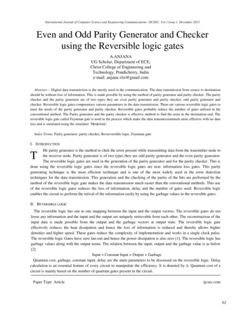
International Journal of Computer Science and Engineering Communications- IJCSEC. Vol.1 Issue.1, December 2013The calculation of the Quantum cost is done by using the gate whose quantum cost is known and finally adding up allthe quantum cost of the gates present in the circuit [3]. Each and every gate produces the output which is not used forthe further synthesis and those left out outputs are called the ‘garbage’. Although the garbage values are not used forthe further synthesis they are essential to achieve the reversibility. The constant inputs are the 0’s and 1’s. The constantinput terms are also called as ancilla input bit [4].Fig. 1. Reversible Feynman GateThe reversible logic gate used in this paper is the Feynman gate and this gate has the quantum cost of about 1.III. PARITY GENERATORParity bits are extra signals which are added to a data word to enable error checking. There are two types of Parity even and odd. An even parity generator will produce a logic 1 at its output if the data word contains an odd number ofones. If the data word contains an even number of ones then the output of the parity generator will be low.A00001111B00110011C01010101OUTPUT (P)01101001Table. 1. Even parity generator truth tableThe truth table for the odd parity generator bit is given by the table below:A00001111B00110011C01010101OUTPUT (P)10010110Table. 2. Odd parity generator truth table63
International Journal of Computer Science and Engineering Communications- IJCSEC. Vol.1 Issue.1, December 2013By concatenating the Parity bit to the data word, a word will be formed which always has an even number of ones i.e.has even parity. Parity is used on communication links (e.g. Modem lines) and is often included in memory systems. If adata or a word is sent out with even parity, but has odd parity when it is received then the data has been corrupted andmust be resent. As its name implies the operation of an Odd Parity generator is similar but it provides odd parity. Evenparity bit is given by the expression P A xor B xor C. The even parity bits generation is given as shown in the abovetables.And the expression for the generation of the odd parity generator is given by P A xor B xor C.The even parity checker is shown in the truth table shown 0110011Pin0101010101010101OUTPUT (P)0110100110010110Table.3 Even parity checker truth tableAnd the expression for the generation of the odd parity generator is given by P A xor B xor C xor Pin.The odd parity checker is shown in the truth table shown 01101010111100110111101111OUTPUT (P)1001011001101001Table. 4. Odd parity checker truth table64
International Journal of Computer Science and Engineering Communications- IJCSEC. Vol.1 Issue.1, December 2013And the expression for the generation of the odd parity generator is given by P A xor B xor C xor Pin.IV. SIMULATION AND DISCUSSIONThe output of the even and odd parity generator and the parity checker is obtained by using the ‘Modelsim’ Simulatoris as given below:Fig. 2. Even parity generator simulationFig. 3. Odd parity generator simulationParitygeneratorEvenNumber ofFeynman gates16Garbagevalue16Odd241665
International Journal of Computer Science and Engineering Communications- IJCSEC. Vol.1 Issue.1, December 2013Fig. 4. Even parity checker simulationFig. 5. Odd parity checker simulation.Parity checkerNumber of Feynman gatesGarbage valueEven4848Odd6448V. CONCLUSIONThus the retiving of the data from the input data is made easy and more efficient while performing wit the reversiblelogic gates. The use of Feynman gate for parity generator and the parity checker with reduced power dissipation. Theretival of the input data from the output so generated is made highly possible by the use of the garbage values.Hencereversible logic gates are effective than the conventional methods for efficient data transmission. The loss ofinformation is zero in case of using the reversible logic gates for the data transmission in the digital form.REFERENCES[1] Madhusmita Mahapatro, Sisira Kanta Panda, Jagannath Satpathy, Meraj Saheel, M.Suresh, Dr. Ajit Kumar Panda, M K Sukla,“Design of Arithmetic Circuits Using Reversible Logic Gates and Power Dissipation Calculation,” 2010 International Symposiumon Electronic System Design.[2] Dmitri Maslov,Gerhard W.Dueck, “Garbage in Reversible Designs of Multiple Output Functions,”Research supported by theNSERC (CANADA).[3] Anindita Banerjee and Anirban Pathak, “An Algorithm for Minimization of Quantum Cost,”Appl. Math. Inf. Sci. 6, No. 1, 157-165(2012) / www.naturalspublishing.com/amis/.[4] Himanshu Thapiliyal, Nagarajan Ranganathan, “Design of Efficient Reversible Logic Based Binary and BCD Adder Circuits,”ACM Journal on Emerging Technologies in Computing Systems Vol. V, No. N, Month 20YY.66
Parity checker Number of Feynman gates Garbage value Even 48 48 Odd 64 48 V. CONCLUSION Thus the retiving of the data from the input data is made easy and more efficient while performing wit the reversible logic gates. The use of Feynman gate for parity generator and the parity checker with reduced power dissipation. The