Transcription
research papersISSN 1399-0047A high-transparency, micro-patternable chip forX-ray diffraction analysis of microcrystals undernative growth conditionsThomas D. Murray,a,b Artem Y. Lyubimov,c Craig M. Ogata,d Huy Vo,e MonarinUervirojnangkoorn,c Axel T. Brungerc* and James M. Bergerb*Received 10 April 2015Accepted 11 August 2015Edited by E. F. Garman, University of Oxford,EnglandKeywords: microcrystals; silicon nitride; serialdata collection; XFEL; microfocus beamline;X-ray crystallography; microfluidics.PDB reference: hen egg-white lysozyme, 4z98Supporting information: this article hassupporting information at journals.iucr.org/daBiophysics Graduate Group, University of California, Berkeley, CA 94720, USA, bDepartment of Biophysics andBiophysical Chemistry, Johns Hopkins University School of Medicine, Baltimore, MD 21205, USA, cDepartments ofMolecular and Cellular Physiology, Neurology and Neurological Sciences, Structural Biology and Photon Science, andHoward Hughes Medical Institute, Stanford University, Stanford, CA 94305, USA, dGM/CA@APS, X-Ray ScienceDivision, Advanced Photon Source, Argonne National Laboratory, Argonne, IL 60439, USA, and eDepartment ofBiomedical Engineering, Johns Hopkins University, Baltimore, MD 21205, USA. *Correspondence e-mail:brunger@stanford.edu, jberge29@jhmi.eduMicrocrystals present a significant impediment to the determination ofmacromolecular structures by X-ray diffraction methods. Although microfocussynchrotron beamlines and X-ray free-electron lasers (XFELs) can enable thecollection of interpretable diffraction data from microcrystals, there is a need forefficient methods of harvesting small volumes ( 2 ml) of microcrystals grownunder common laboratory formats and delivering them to an X-ray beam sourceunder native growth conditions. One approach that shows promise inovercoming the challenges intrinsic to microcrystal analysis is to pair so-called‘fixed-target’ sample-delivery devices with microbeam-based X-ray diffractionmethods. However, to record weak diffraction patterns it is necessary tofabricate devices from X-ray-transparent materials that minimize backgroundscattering. Presented here is the design of a new micro-diffraction deviceconsisting of three layers fabricated from silicon nitride, photoresist andpolyimide film. The chip features low X-ray scattering and X-ray absorptionproperties, and uses a customizable blend of hydrophobic and hydrophilicsurface patterns to help localize microcrystals to defined regions. Microcrystalsin their native growth conditions can be loaded into the chips with a standardpipette, allowing data collection at room temperature. Diffraction data collectedfrom hen egg-white lysozyme microcrystals (10–15 mm) loaded into the chipsyielded a complete, high-resolution ( 1.6 Å) data set sufficient to determine ahigh-quality structure by molecular replacement. The features of the chip allowthe rapid and user-friendly analysis of microcrystals grown under virtually anylaboratory format at microfocus synchrotron beamlines and XFELs.1. IntroductionX-ray crystallography has long aided researchers in determining the high-resolution structures of biological macromolecules and their complexes. Although widespread in theiruse and utility, crystallographic efforts to obtain structuralinformation are frequently hampered by an inability to obtainlarge, well diffracting crystals. Indeed, microcrystals ( 15 mmin the longest dimension) are often found during initial searches for crystallization conditions, and in many instancesprojects can stall in proceeding beyond the microcrystal limit.The challenge of working with microcrystals has spurred thedevelopment of technical innovations aimed at overcomingthe weak diffraction and radiation-sensitivity inherent tomicrometre-sized samples. In recent years, advances such asmicrofocus synchrotron beamlines and X-ray free-electronlasers (XFELs) have made it possible to collect usefulActa Cryst. (2015). D71, 50111987
research papersdiffraction data from a variety of microcrystalline systems(Boutet et al., 2012; Chapman et al., 2006, 2011; Cowan &Nave, 2008; Cusack et al., 1998; Finfrock et al., 2010; Fischettiet al., 2009, 2013; Hilgart et al., 2011; Johansson et al., 2012;Moukhametzianov et al., 2008; Perrakis et al., 1999; Sanishviliet al., 2008, 2011; Sawaya et al., 2014; Smith et al., 2012).Although beamline technologies can presently work withcrystals in the submicrometre size regime (Chapman et al.,2011), sample harvesting and targeting remain two persistentdifficulties associated with microcrystal diffraction studies. Forexample, with XFELs, liquid-jet injection systems can be usedto continuously flow a thin stream of microcrystals into thepath of a rapidly pulsing X-ray beam (DePonte et al., 2008;Sierra et al., 2012; Weierstall et al., 2012, 2014). Liquid jetshave successfully been used in several structural analyses(Barends et al., 2014; Botha et al., 2015; Boutet et al., 2012;Chapman et al., 2011; Johansson et al., 2013; Kern et al., 2012,2013, 2014; Kupitz et al., 2014; Liu, Wacker et al., 2013;Redecke et al., 2013); however, these devices also have anintrinsically low ‘hit’ rate (i.e. a low number of ‘beam-ontarget’ events compared with the total number of exposurescollected) and they tend to consume large sample volumes(hundreds of microlitres to tens of millilitres) during thecourse of an experiment (Boutet et al., 2012; Chapman et al.,2011; Sierra et al., 2012; Weierstall et al., 2014). Capillary-basedliquid-stream systems, which have successfully been used withmicrofocus synchrotron beamlines (Stellato et al., 2014), havesimilarly large sample requirements.‘Fixed-target’ devices for delivering microcrystals constitutea valuable alternative to liquid-jet systems (Cohen et al., 2014;Hirata et al., 2014). Loops, micromeshes or polycarbonateplastic grids offer low volume consumption and relatively hightarget hit rates (Cohen et al., 2014; Hirata et al., 2014), a usefulfeature in instances when crystalline material is limiting.Despite these beneficial properties, fixed-target devices arenot without their own drawbacks. For example, crystalsdeposited onto plastic meshes require cryopreservation toavoid dehydration; the search for suitable cryoprotectionconditions is often difficult, and in some cases the change insolutes or the cooling process itself can adversely reduce thecrystalline order or affect the protein structure (Fraser et al.,2009, 2011; Keedy et al., 2014; Tilton et al., 1992). Some fixedtarget delivery systems, such as MiTeGen MicroRT capillarymounts, PDMS-based microfluidic devices (Heymann et al.,2014; Khvostichenko et al., 2014; Lyubimov et al., 2015), siliconnitride grids (Frank et al., 2014; Hunter et al., 2014; Kimura etal., 2014), the HC1 humidity-control device (Sanchez-Weatherby et al., 2009) and polyimide (Kapton) film-based grids(Cipriani et al., 2012; Zarrine-Afsar et al., 2012) can circumvent problems associated with cryoprotection by permittingsample analysis at room temperature. Furthermore, microfluidic devices can allow the growth or capture of microcrystalsfrom dilute solutions within addressable arrays (Hansen et al.,2002, 2006; Heymann et al., 2014; Khvostichenko et al., 2014;Lyubimov et al., 2015; Zheng et al., 2004).One disadvantage that some fixed-target approaches suffercompared with liquid-jet devices is an increase in background1988Murray et al. High-transparency, micro-patternable chipscatter that arises from the device material. For example,PDMS gives rise to a sharp scattering ring at 7.5 Å resolution (Dhouib et al., 2009; Greaves & Manz, 2005; Guha et al.,2012) and device fabrication typically requires relatively thick( 50 mm) material layers, properties that can interfere withweak diffraction patterns (Hansen et al., 2006; Lyubimov et al.,2015). Silicon nitride supports offer relatively low backgroundscatter and high X-ray transmission compared with PDMS(Frank et al., 2014; Hunter et al., 2014), but microcrystalharvesting devices of this type reported thus far have relied onloading schemes that remove samples from their native growthconditions (Feld & Frank, 2014; Frank et al., 2014; Hunter etal., 2014), a step that can adversely impact diffraction quality.The HC1 humidity-control device allows room-temperaturedata collection through user-controllable partial dehydrationof crystalline samples on thin mounts; however, the systemrequires that optimized crystals be cryocooled for full data-setcollection (Sanchez-Weatherby et al., 2009). For their part,polyimide (Kapton) film based-devices have been describedthat exhibit low scattering and that can maintain nativecrystal-growth conditions during loading (Cipriani et al., 2012;Zarrine-Afsar et al., 2012); however, these systems have eitherrequired that crystals be grown in the device (Cipriani et al.,2012) or that large glass beads (Zarrine-Afsar et al., 2012)whose dimensions are much larger (up to 100 mm) than thoseof the microcrystals be used to create a textured surface forrandomizing the crystal orientation (Zarrine-Afsar et al.,2012).To begin to overcome some of the limitations present incurrent fixed-target devices, a new silicon nitride-based chipthat permits the collection of X-ray diffraction data frommicrocrystals under native growth conditions has beendeveloped. Using a combination of high X-ray transmissionmaterials, including silicon nitride, Kapton film and patternable photoresist, the chip is capable of accepting a smallvolume ( 2 ml) of microcrystalline slurry from a standardpipette, confining it within a defined imaging area and favorably biasing the positions of single microcrystals with micropatterned features. These chips were used to collect X-raydiffraction data under an XFEL-like, zero-oscillation, ‘onecrystal/one-shot’ strategy from 10–15 mm-sized hen eggwhite lysozyme (HEWL) crystals on microfocus beamlinesusing manual targeting. This approach allowed the collectionof a complete, high-quality (1.55 Å resolution) data set from 325 microcrystals, Additionally, test exposures of HEWLmicrocrystals using an X-ray free-electron laser (XFEL)produced high-quality diffraction data, demonstrating theutility of the chips for use with either microfocus synchrotronor XFEL X-ray radiation.2. Materials and methods2.1. Chip fabrication100 mm diameter, 525 ( 25) mm thick ‘prime’-grade siliconwafers coated with 1500 Å ( 5%) of low-pressure, chemicalvapor-deposited silicon nitride (WRS Materials) were used tofabricate silicon nitride windows for all device designs. WafersActa Cryst. (2015). D71, 1987–1997
research paperswere dehydration-baked at 200 C for 60 min and, followingcooling, were patterned with 2 mm thick S1813 photoresist(Dow) into the desired arrays using a laser-etched chromemask (Front Range PhotoMask) and standard photolithography techniques (Jaeger, 2002). S1813 photoresist was spunonto the back side of the wafer to a thickness of 2 mm toprotect the silicon nitride layer on the back side duringsubsequent deep reactive ion etching (DRIE) treatment.Following a 115 C bake to harden the photoresist on the backside of the wafer, the wafer underwent DRIE using carbontetrafluoride (CF4) plasma to selectively remove silicon nitridethat was exposed from the previous transfer of the desiredwindow pattern. The photoresist was then stripped off in anacetone bath and the wafer was then dunked into a 90 C30%(w/v) potassium hydroxide bath for wet etching of thesilicon wafer. The wet etch proceeded at a rate of roughly1 mm min 1 and, following its completion, the wafer was thenrinsed thoroughly with deionized water. To prepare the waferfor photoresist patterning of the middle layer, the wafer wasdehydration-baked at 200 C for 60 min and was then oxygenplasma-treated (300 W for 5 min) using a PEII-A plasma etchchamber (Technics). SPR 220-7.0 photoresist (Dow) wassubsequently spun onto the continuous silicon nitride surfaceside of the wafer to a height of 15 mm for channel chip designs,or SPR 220-3.0 (Dow) was spun to a height of 5 mm onto thewafer for photoresist-stripe chip designs. The photoresistfeatures were patterned using standard photolithographytechniques and a laser-etched chrome mask (Front RangePhotoMask). To render the photoresist stripes hydrophilic, thephotoresist was oxygen plasma-treated using an Atomflo 400series plasma generator (Surfx). Individual devices wereexcised from the wafer using a diamond-tipped pen to applypressure along dice lines that were patterned onto the waferalong with the initial window array and etched into the waferduring wet etching.2.2. Crystal growth and chip loading for optical imaging ofmicrocrystals within silicon nitride chipsHen egg-white lysozyme (HEWL) microcrystals weregrown as described by Falkner et al. (2005), except that acommercially available preparation of HEWL (OmniPure,5950-OP) was used and the crystal cross-linking step wasomitted. Lyophilized lysozyme was resuspended at 20 mg ml 1in sodium acetate pH 3.5 and split into 50 ml aliquots that werethen stored at 20 C. For crystallization, the lysozyme solution was thawed and then spun for 10 min at 13 000 rev min 1in a bench-top centrifuge (Eppendorf 5424) to remove anyprecipitate or fine-particulate matter. The clarified solutionwas then transferred to a fresh microcentrifuge tube andcrystallization buffer was added at a 1:3 (protein:buffer) ratio.To generate crystals of 10–15 mm in size, a 20% sodiumchloride, 8%(w/v) poly(ethylene glycol) 8000, 0.5 M sodiumacetate pH 3.5 solution was used. Crystals formed within15 min when the solution was placed on ice or in a 4 C coldroom.For optical imaging of chips loaded with HEWL microcrystals, the microcrystalline slurry was first agitated byActa Cryst. (2015). D71, 1987–1997pipetting the mixture up and down. Next, 0.5 ml of thispreparation was spotted on top of a photoresist-patternedsilicon nitride window. For covering chips, a piece of 8 mmthick Kapton film (SPEX SamplePrep, catalog No. 3511) ofsufficient dimensions to cover all silicon nitride observationwindows was cut using a razor blade and placed on top of thesolution. Images of crystals on the chip were taken using anOlympus IX71 microscope fitted with a Retiga 2000R camera(Q Imaging).For X-ray data collection on Stanford Synchrotron Radiation Laboratory (SSRL) beamline BL12-2 and the X-rayPump Probe (XPP) endstation of the Linac Coherent LightSource (LCLS), chips were loaded and covered as describedfor optical imaging. At the Advanced Photon Source, 0.5 mlfreshly prepared HEWL microcrystal slurry was pipetted ontofour consecutive windows, as only four windows were accessible for data collection on each silicon nitride chip owing tothe geometry of the mounting devices and beamline endstation.2.3. Diffraction data collection and crystal structuredeterminationBackground-scattering X-ray diffraction experiments wereperformed on SSRL beamline BL12-2 with a 10 mm beam, 3 sexposures and 0.02 oscillations. X-ray diffraction experimentson 10–15 mm HEWL microcrystals used a 10 mm beam, 5 sexposures and 0.02 oscillations. Images were collected on aDectris PILATUS 6M detector. 5 30 mm channel-basedchips (Supplementary Fig. S1) were used for all measurements.A custom-made chip mount was used for all experiments.Crystals positioned either entirely on a silicon nitride surfaceor entirely on a photoresist-coated silicon nitride surfaceproduced diffraction without any noticeable differences(Supplementary Fig. S2). Both diffraction images weresubsequently indexed with the expected space group and unitcell parameters for tetragonal HEWL microcrystals (P43212,a b 79.1, c 38.1 Å, 90.0 ).X-ray diffraction experiments were performed using 10–15 mm HEWL microcrystals at the XPP endstation of theLCLS with a 3 mm unattenuated beam and 40 fs pulses. Testexposures of 5 30 mm channel-based chips (SupplementaryFig. S1) were taken using either 40 fs pulses of a 3 mm unattenuated beam (Supplementary Figs. S3a, 4a and 4b) or a30 mm unattenuated beam (Supplementary Figs. S4c and S4d)at 9 keV. Still (zero-oscillation) images were collected on aRayonix MX325 detector. 5 30 mm channel-based chips(Supplementary Fig. S1) and a custom-made chip mount (astandard magnetic base with a machined chip-holding slot)were used for all measurements. The detector was positionedsuch that the corner corresponded to a resolution of 2.0 Å.Using JBluIce–EPICS (Stepanov et al., 2011), crystals weremoved into the beam by first focusing on a single 1 mm2 siliconnitride window at low magnification. Subsequently, themagnification was increased to such a level that individualmicrocrystals could clearly be seen, and a single microcrystalwas then manually targeted for exposure.Murray et al. High-transparency, micro-patternable chip1989
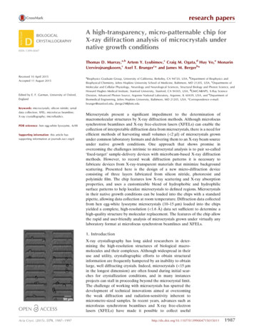
research papersCollection of a full data set tookplace on the The General MedicalSciences and Cancer Institutes Structural Biology Facility (GM/CA) beamline 23-ID-D at the Advanced PhotonSource (APS) using a zero-oscillation,serial data-collection strategy with a10 mm diameter beam and a PILATUS36M detector. Chips were mounted usinga custom-made chip holder developedat GM/CA. A total of 324 (0.25 sexposure) images were collected during 8 h of beamtime. Eight chips wereused for data collection, with chipsgenerally remaining mounted andunder observation for 30–60 min induration; one chip was examined for107 min. HEWL microcrystals werelocated by eye by manually rasteringfrom the upper left-hand to lower righthand corner of a silicon nitride window.Figure 1Three-layer device layout. (a) Schematic representation of chip layers. (b) Cut-away view of theAfter exposing crystals within a singleimaging chamber of the assembled chip with a 150 nm thick silicon nitride window, 15 mm thickwindow, the chip was translated to thephotoresist and 8 mm thick Kapton film layer. (c) 100 mm diameter wafer patterned with 24 5 adjacent window, and this window was30 mm devices. (d) Photograph of a single 5 30 mm device (silicon nitride layer only).also rastered manually. Hydrophilictransparent materials and the middle layer is configured as aphotoresist stripe-based chips (10 30 mm device dimensions,separating support layer that also helps to trap microcrystalstripe-patterned) were used in these experiments.line samples (Figs. 1a and 1b). Silicon nitride was selected asTo establish the minimum X-ray dose necessary forthe foundation material for the chip owing to its low cost andmaximum-resolution data-set collection, a single HEWLits established utility in diffraction experiments (Feld & Frank,microcrystal was first subjected to a series of ten 1.0 s expo2014; Frank et al., 2014; Hunter et al., 2014; Kimura et al.,sures of radiation to determine the time at which the diffrac2014). After consulting with staff scientists at the SSRL, thetion resolution limit began to decrease. After a singleAPS and the LCLS about desirable dimensions, a series ofmicrocrystal survived only one 1.0 s exposure, a lower doserectangular (5 30 mm) ‘chips’, which feature an array of tenseries of ten 0.3 s exposures were performed on another single1 mm2 150 nm thick silicon nitride observation windows,microcrystal. The resolution decreased during the second 0.3 swere fabricated. For high fabrication efficiency, patterningexposure. After ten 0.1 s exposures revealed that the resolumasks that allow up to 24 such devices to be generated from ation limit did not extend to the edge of the detector, a 0.25 ssingle 100 mm diameter silicon nitride-coated silicon waferexposure was chosen for data-set collection.were created (Figs. 1c and 1d). Photoresist was chosen as aA total of 324/324 (0.25 s exposure) diffraction images weremiddle, supporting layer owing to its patternability andindexed and integrated using the cctbx.xfel software suitefavorable X-ray transmission properties (Dhouib et al., 2009;(Hattne et al., 2014). PRIME was then used to successfullyWells, 1992). Commercially available 8 mm thick polyimidemerge, scale and post-refine 324/324 of the integrated images(Kapton) film was selected as the top layer for its low air(Uervirojnangkoorn et al., 2015). The lysozyme structure waspermeability, frequent use in X-ray diffraction experimentsdetermined by molecular replacement using Phaser (McCoy et(Cipriani et al., 2012; Heymann et al., 2014; Zarrine-Afsar etal., 2007) and refined using phenix.refine (Adams et al., 2010),al., 2012) and durability.while manual rebuilding and adjustment was carried out inPhotoresist patterning is highly tunable, allowing structuresCoot (Emsley et al., 2010). Rfree-flagged reflections wereof virtually any shape to be constructed on a surface throughwithheld from all output maps, beginning with the molecularstandard photolithography (Jaeger, 2002). To help to confinereplacement maps.and position protein microcrystals, the photoresist (middle)layer was initially patterned into a series of long parallel3. Resultschannels. The channels were designed to be 20 mm wide and3.1. Construction of a three-layer silicon nitride-based chip15 mm tall (corresponding to a set of dimensions somewhatfor harvesting protein microcrystalslarger than a typical microcrystal), separated by 50–100 mmwide photoresist walls and of a length that either spanned theTo construct a platform for microcrystal X-ray diffractionentirety of the 1 mm2 silicon nitride window (Supplementaryexperiments, a three-layer chip was designed in which theFig. S1a) or that was divided into two 0.5 mm segmentstop and bottom segments are composed of highly X-ray-1990Murray et al. High-transparency, micro-patternable chipActa Cryst. (2015). D71, 1987–1997
research papers(Supplementary Fig. S1b). The relative channel-to-channelspacing was also varied in early prototypes of our chips(Supplementary Figs. S1c and S1d), although neither variationin channel length nor in channel spacing was subsequentlyfound to affect chip performance (not shown).To test the channel-based chip designs, 0.5 ml of a hen eggwhite lysozyme (HEWL) microcrystalline slurry ( 10–15 mmaverage crystal size) was pipetted atop a photoresist-patternedsilicon nitride window and the sample was covered with asingle strip of Kapton film. Following the placement of theKapton film layer, the crystals did indeed settle into thepatterned channels (Fig. 2a). However, crystals frequentlyresided on the topmost surface of the photoresist, sandwichedbetween this layer and the Kapton film (Fig. 2b). Althoughtest exposures did not reveal any appreciable increase inbackground scattering from chip areas that contained photoresist versus those that did not (Supplementary Fig. S2), thechips were redesigned in such a way that the crystals wouldfavor either an association with the silicon nitride directly orwith the edges of the photoresist features, so that the Kaptonfilm did not press them into the photoresist.3.2. Hydrophilic surface patterning improves microcrystallocalizationBased on the initial finding that crystals tended to associatewith the upper, flat surface of the photoresist as readily as withthe silicon nitride flooring of the patterned channels, theinnately hydrophobic nature of both layers appeared to bepreventing any preferential localization to one material or theother. This idea suggested that a relatively hydrophilic surfaceto which protein microcrystals could become stably anchoredmight be beneficial. To overcome the hydrophobicity of theentirety of the chip, an oxygen plasma treatment was used torender the photoresist layer hydrophilic (Northen & Turner,2005; Walther et al., 2007). A more textured surface to the chipwas introduced by patterning denser numbers of photoresiststructures onto the silicon nitride layer; such an approach hasbeen shown to aid surface wetting (Marinaro et al., 2014;Zarrine-Afsar et al., 2012) and to help to randomize theorientation of samples deposited on a surface (Zarrine-Afsaret al., 2012).Firstly, an array of rectangular photoresist stripes of varyingdimensions and spacings was designed (Fig. 3). Stripes were20 mm in width, and ranged from the length of the windowto 150 mm in length. Following photoresist patterning andoxygen plasma treatment, light microscopy was used to assesswhether microcrystals would preferentially associate with theedges of the treated photoresist stripes compared withuntreated stripes. 0.5 ml of a freshly prepared HEWL microcrystal slurry was loaded onto a photoresist stripe-patternedsilicon nitride window, covered with Kapton film and thenumber of observable crystals within the bounds of the 1 mm2silicon nitride observation window was then counted (Figs. 4aand 4b). HEWL microcrystals showed a clear preference forlocalizing to the long edges of hydrophilic photoresist stripes(Fig. 4c), indicating that that the features were indeed usefulfor biasing microcrystal placement. The more texturedphotoresist structures also appeared to help to randomize theorientation of microcrystals within the chip (Fig. 4d).3.3. X-ray diffraction studies of microcrystals deposited insilicon nitride chipsFigure 2Optical imaging of loaded channel-based chips. (a, b) Light micrographsof sealed three-layer chips designed with 20 mm wide channels and loadedwith 10–15 mm HEWL microcrystals.Acta Cryst. (2015). D71, 1987–1997To test the performance of the chips, they were assessed onthe BL12-2 microfocus beamline at the SSRL using a mountderived from a standard crystal loop magnetic base. X-raydiffraction experiments were also conducted at the APS usinga custom-built chip mount intended to hold devices of varioussizes (Fig. 5a) and at the XPP endstation of the LCLS using amodified magnetic base compatible with a standard goniometer (Fig. 5b). The rigid nature of the chips allowed efficientmounting using a variety of custom-made holders in theconfined space of a goniometer setup. The low total chamberthickness ( 25 mm; Fig. 1b) and optical transparency of thechips also allowed easy identification and targeting of crystalsMurray et al. High-transparency, micro-patternable chip1991
research paperspositioned within a silicon nitride observation window duringdata collection, even when the device was tilted by up to 45 .As anticipated, the three-layer chips exhibited very lowbackground signal (Fig. 6a). The levels of background scatterproved to be much lower than that of a PDMS-based microfluidic crystal-capture device (Figs. 6b and 6c), with the onlyprominent background feature being a scattering ring generated by the Kapton film at 16 Å (Figs. 6a and 6c). The chipswere next tested using 10–15 mm-sized HEWL microcrystalson BL12-2 at SSRL (Supplementary Fig. S2), the LCLS XPPendstation (Supplementary Fig. S3a) and GM/CA beamline23-ID-D at the APS (Supplementary Fig. S3b). In eachinstance, the resultant diffraction images indexed with thespace group (P43212) and unit-cell parameters (a b 79.1,c 38.1 Å, 90 ) commonly observed for tetragonalHEWL crystals. Moreover, high-resolution data were clearlyevident in the diffraction pattern, with diffraction maximafrequently seen extending to 1.5 Å resolution (Supplementary Fig. S3b), compared with the 1.8 Å resolution spots thatwere occasionally observed from thin-layer PDMS chips(Lyubimov et al., 2015).3.4. Structural validation of chip performanceHaving established that the three-layer silicon nitride-basedchips allow the collection of high-resolution diffraction data, acomplete diffraction data set was collected using the devicesat room temperature. Diffraction images were collected onGM/CA beamline 23-ID-D at the APS using 10–15 mm-sizedHEWL microcrystals and a 10 mm diameter beam size. Totaldata-collection times often reached 1 h per chip, with thelongest duration being 107 min from the first to last exposure;this amount of time proved to be more than sufficient to allowall segments of a chip to be used before the samples dehydrated. One zero-oscillation (‘still’) diffraction image percrystal was taken to approximate an XFEL-like serial datacollection experiment. Prior to data collection, the minimalX-ray exposure time (0.25 s) that would still yield maximumFigure 3Photoresist stripe-based chip designs. (a, b, c) Schematic representation of the design masks for patterning a 1 mm2 silicon nitride window with 20 mmwide photoresist structures of varying lengths. (d) Optical micrograph of an area within a single 1 mm2 silicon nitride window patterned with 20 mm wideby 137.5 mm long photoresist structures.1992Murray et al. High-transparency, micro-patternable chipActa Cryst. (2015). D71, 1987–1997
research papersdiffraction resolution for these crystals was determined (x2.3,Materials and Methods). This exposure time corresponds toapproximately 0.05–0.1 times the number of 8 keV photonsdelivered in a single FEL pulse. Chip tilts ( 44 in 2 increments) were used during collection to ensure that all regionsof reciprocal space were appropriately sampled; in this regard,the hydrophilic and textured features of the photoresistproved valuable in randomizing microcrystal orientation,thereby allowing a complete serial X-ray diffraction data set tobe collected from a relatively small ( 325) number of microcrystals (Supplementary Fig. S5). The final data set wasassembled from 324/324 of the still images acquired from eightphotoresist stripe-patterned chips (Fig. 3). Interestingly, individual images often indexed and integrated to 1.3 Å resolution, demonstrating the high signal-to-noise properties ofthe chips (Supplementary Fig. S6).Following data collection, cctbx.xfel (Hattne et al., 2014) wasused for indexing and integration of diffraction images andPRIME (Uervirojnangkoorn et al., 2015) was used for scaling,merging and post-refinement. A total of 324 indexed/integrated diffraction images resulted from this process. Themerged data set was 91.6% complete in th
window pattern. The photoresist was then stripped off in an acetone bath and the wafer was then dunked into a 90 C 30%(w/v) potassium hydroxide bath for wet etching of the silicon wafer. The wet etch proceeded at a rate of roughly 1 mmmin1 and, following its completion, the wafer was then rinsed thoroughly with deionized water. To prepare the wafer