Transcription
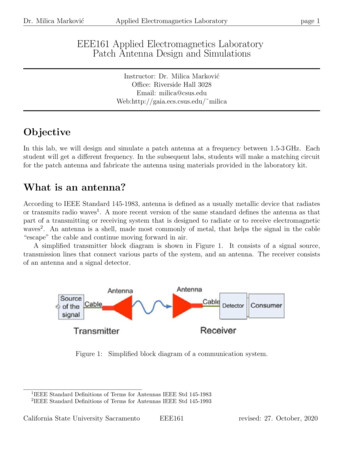
Dr. Milica MarkovićApplied Electromagnetics Laboratorypage 1EEE161 Applied Electromagnetics LaboratoryPatch Antenna Design and SimulationsInstructor: Dr. Milica MarkovićOffice: Riverside Hall 3028Email: milica@csus.eduWeb:http://gaia.ecs.csus.edu/ milicaObjectiveIn this lab, we will design and simulate a patch antenna at a frequency between 1.5-3 GHz. Eachstudent will get a different frequency. In the subsequent labs, students will make a matching circuitfor the patch antenna and fabricate the antenna using materials provided in the laboratory kit.What is an antenna?According to IEEE Standard 145-1983, antenna is defined as a usually metallic device that radiatesor transmits radio waves1 . A more recent version of the same standard defines the antenna as thatpart of a transmitting or receiving system that is designed to radiate or to receive electromagneticwaves2 . An antenna is a shell, made most commonly of metal, that helps the signal in the cable“escape” the cable and continue moving forward in air.A simplified transmitter block diagram is shown in Figure 1. It consists of a signal source,transmission lines that connect various parts of the system, and an antenna. The receiver consistsof an antenna and a signal detector.Figure 1: Simplified block diagram of a communication system.12IEEE Standard Definitions of Terms for Antennas IEEE Std 145-1983IEEE Standard Definitions of Terms for Antennas IEEE Std 145-1993California State University SacramentoEEE161revised: 27. October, 2020
Dr. Milica MarkovićApplied Electromagnetics Laboratorypage 2Types of antennasSome of the most common antennas are shown in Figure 2.(a) Horn(b) Dipole(c) Yagi-Uda(d) Helix(e) Loop(f) DishFigure 2: Antenna types.Antenna Vocabulary1. 377-Ω transmission line. Free space can be represented as a 377-Ω transmission line.2. Near-Field Antennas3. Far-Field. A communication system that employs one of the antennas mentioned is made totransmit the signal at large distances through the air. In order to efficiently transmit signals,transmitting and receiving antennas have to be separated by a minimal distance. This minimumdistance between two antennas and be calculated using Equation 1. In today’s experiment, youwill first have to calculate this minimum distance as given byF F 2d2 /λ(1)Where d is the maximum size of the antenna. For a horn antenna, this is the length betweentwo opposite corners of the largest rectangular opening. λ is the wavelength of the signal andCalifornia State University SacramentoEEE161revised: 27. October, 2020
Dr. Milica MarkovićApplied Electromagnetics Laboratorypage 3is calculated as λ c/f . c is the speed of light 3 108 m/s, and f is the frequency of the signalin Hz.4. Antenna Pattern. antenna radiates most power in a certain direction in space. The exactdistribution of this power in space is called the antenna pattern. We will measure this antennaproperty in the lab today. This property of an antenna is usually drawn on the x-y plane aspower (on the y-axis) as a function of degrees away from the antenna axis, as shown in Figure3.Figure 3: Example of Antenna’s radiation pattern.5. Antenna Beam. The shape of the radiated power in 3-D space looks like a beam, and it iscalled an antenna beam.6. Beam-width. Beamwidth is the measure of the antenna beam in degrees. It shows how manydegrees away from the axis of the antenna most power is concentrated in. We define the pointat which the beamwidth in degrees is calculated as the point where the antenna power fallsoff to 0.5 of the maximum power (or if you measure the voltage on the oscilloscope, then find0.707 point).7. Directivity. Directivity is the measure of the narrowness of the antenna beams. The higherthe directivity, the narrower the beam is. The formula to estimate directivity isD 4πβxy βyz(2)βxy is the beamwidth in the XY plane and βyz in the beamwidth in the perpendicular plane.Both βs need to be converted to radians first. Directivity is usually quoted in decibels. To finddirectivity in decibels, use the formula below:DdB 10log(D)(3)Patch antenna designPatch antenna consists of a patch of metal on a dielectric substrate backed by metal ground, asshown in Figure 4.California State University SacramentoEEE161revised: 27. October, 2020
Dr. Milica MarkovićApplied Electromagnetics Laboratorypage 4The two features of a patch antenna are a width W and a length L. The length L represents thedistance between two radiating resonant edges. These edges are also called radiating slots becausethe slot between the ground and the metal on top is what radiates in this antenna. Blue arrowsare pointing blue ovals that encircle radiating slots (resonant edges). The width W separates twononresonant edges and represents the width of the radiating slot. The top side of the antenna shouldnot be too close to the edge of the board. If your antenna is large, you may not have a choice, butif you do have a choice, move it away from the edge of the board as much as you can.You can also see in Figure 4 a fully transmission-line impedance matching circuit for the antennawith an open stub. All (red) microstrip lines on this board have the same transmission-line impedanceZ0 (the same width), but different lengths. The length of the line that separates the antenna fromthe stub is labeled as ”d,” and the length of the stub is labeled as ”s.” The stub ”s” and lines ”d” and”a” meet at a point where three lines make a ”Tee.” At that point, the impedance looking towardsthe antenna is equal to transmission-line impedance Z0 . We made this input impedance equal to Z0with the transmission-line impedance matching circuit. The reflection coefficient at this point is zerobecause the transmission line ”a”’s impedance is Z0 , and it is terminated with the load Z0 . Sincethe reflection coefficient at the end of the line ”a” is zero, the line can be any length.It is important that the stub ”s” is not close to the edge of the board. As a rule of thumb, theboard edge must be at least five widths of the stub away.Finally, at the very bottom of the figure, you can observe the top side of an SMA connector. The(green) line ”a” is soldered to the connector. Care must be taken that the line ”a” does not touchthe nuts on this side of the board, as this will ”short” the line ”a” to the ground and all the powercoming from the generator will reflect back to the generator, so no power will reach the antenna.Design SpecificationsThe substrate we will be using is polycarbonate. The electric permittivity r 3, and it may varyfrom 2.5-3. The height of the board is 1/8 inch. The frequency of operation fr will be assigned bythe instructor, and it will be between 1.5-2.9 GHz.Patch antenna design processTo design a patch antenna, we use the steps described below. The equations to use in these stepsare given in the section ”Calculation of patch antenna dimensions.”1. Calculate the optimal patch antenna width W to make the patch an efficient radiator.2. Determine the effective dielectric constant ef f .3. Determine the extension of the length L.4. Find the actual length of the patch L.California State University SacramentoEEE161revised: 27. October, 2020
Dr. Milica MarkovićApplied Electromagnetics Laboratorypage 5Figure 4: Example patch antenna made by Prof. Rucker.Calculation of patch antenna dimensionsTo find the length and width of the patch, we use the following equations:c 2 L2fr ef fr2cW 2fr r 1L (4)(5)To find the extention of the line due to fringing fields L, and effective dielectric constant ef fwe use the following formulas: r 1 r 11q 221 12 h(6) ( ref f 0.3) Wh 0.264 L 0.412h( ref f 0.258) Wh 0.8(7) ref f W(8)California State University SacramentoEEE161revised: 27. October, 2020
Dr. Milica MarkovićApplied Electromagnetics Laboratorypage 6In the above equations, the ef f is the effective dielectric constant. r is the relative dielectric constant of the substrate. The approximate value of the inputimpedance of the resonant-edge fed patch can be calculated as: 2Zin 90 r r 1 LW 2Ω(9)ExampleDesign a 1GHz microstrip antenna using the substrate with a dielectric constant of 3 and substratethickness of 125 mils.Using the equations above, at 1 GHz, effective dielectric constant is ref f 2.857, length correction is L 0.16 cm, the patch antenna length is L 8.56 cm, and the optimal width is W 10.6 cm.The calculated input impedance of the patch is 263.8 Ω. We will now proceed to simulate this antennaand find the simulated input impedance.California State University SacramentoEEE161revised: 27. October, 2020
Dr. Milica MarkovićApplied Electromagnetics Laboratorypage 7Matlab Code to design patch antenna with equations fromthe previous sectionclear allclc%dielectric constant erer 3%frequency f [Hz]f 1*10 9%height of the substrate in inches hin, height in meters hhin 0.125h hin*0.0254%speed of light c [m]c 3*10 8%patch width wW (c/(2*f))*sqrt(2/(er 1))%epsilon effective for the antennaeeff ((er 1)/2) ((er-1)/2)/sqrt(1 12*h/W)%length extension Delta LdeltaL 0.412*h*(eeff 0.3)*(W/h 0.264)/((eeff-0.258)*(W/h 0.8))%length of patch LL (c/(2*f*sqrt(eeff)))-2*deltaL%input impedanceZin 90*er 2*L 2/((er-1)*W 2)Simulation of a patch antenna in HFSSTo find the input impedance exactly, use PATCHFall202050Ohms.aedtz file on Dr. Markovic’s website.Link to archived HFSS project.To open this file, copy it on your T-drive, then open HFSS, and select from the pull-down menuFile- Restore Archive. When you open the workspace, click on thePATCHFall202050Ohmsthen onPatch Antenna ADKv1(DrivenTerminal)to see the Properties window. In the Properties window, change the dimensions of your patchaccording to the calculations above for your frequency. Then change the simulation frequency toyour frequency. Click on HFSS, Analyze All.Dr. Markovic will have a demo of this file and various simulation and visualization tools. At theend of this section, you will have the input impedance of your antenna.California State University SacramentoEEE161revised: 27. October, 2020
Dr. Milica MarkovićApplied Electromagnetics Laboratory(a) Opening HFSS (b) Changingarchived file.the size ofpatch antenna.page 8(c) Changing the frequency of patch antenna.Figure 5: How to open HFSS, and change simulation parameters.Making an impedance matching circuitTo match the antenna to a 50-Ohm generator, you will first make ADS simulations with idealtransmission lines to verify your design, and then with microstrip transmission lines (MLIN) todesign the circuit on the board. Our board has r 3, and the height of the substrate is h 125mils.We don’t have the thickness of the metal, but you can assume 1oz thickness. Follow the steps belowto make the impedance matching circuit for your antenna.1. Open ADS, new schematic. Solve the impedance matching problem using ideal transmissionlines first to give you an idea of what the circuit will look like. Write down the values for theline and stub electrical lengths. When you are done with this step, call the instructor to checkyour circuit. If the circuit is correct, proceed with the next step. In the next step, you willbe designing an actual microstrip line circuit that can potentially be fabricated on the board.Your circuit and results should look like the circuit in Figure 7.2. Go to TLines-Microstrip from the pull-down menu. Select MSUB and place it on the schematic.3. Set the substrate parameters in MSub to what your substrate parameters are.4. Use MLIN for transmission lines, and MLOC for the open-circuited stub, as shown in Figure?. To simulate the effect of Tee junction, we also have to include MTEE where your lines(going to generator and load) and the stub meet. For Microstrip lines, you have to enter theactual width and length of the lines. The width of the line depends mainly on the transmissionline impedance, and the length of the line depends mainly on the electrical length and the typeof substrate.5. Make the impedance-matching circuit look the same as the one you have done with ideal lines.Note that the port impedance (or you could use Eqn-Linear block) on the right must be theCalifornia State University SacramentoEEE161revised: 27. October, 2020
Dr. Milica MarkovićApplied Electromagnetics Laboratory(a) Patch Antenna in HFSS withradiation pattern.page 9(b) Edge fed reflection coefficient of patch antenna.(c) Patch antenna return loss(d) Patch antenna gain.Figure 6: Patch antenna simulation in HFSS.antenna impedance you found from HFSS.6. Now, you have to calculate what the actual width and length of the lines need to be. UseLineCalc for this task. The frequency of operation is your assigned frequency. Note that wemust use the width of the thin copper strip for the line widths. The width of the copper stripis 245mils. This is approximately Z0 57Ω. Check this in LineCalc, and use this width forthe width of your lines.7. When you are done with LineCalc, write the actual values for the Width and Lenght of theline in your circuit.8. Simulate the circuit and make appropriate (minor) changes to the lengths of your lines. DONOT CHANGE THE WIDTH OF THE LINES.9. At this point, you would make a Gerber file for your antenna and matching circuit if we were touse the PCB router to fabricate the circuit. However, we will make the antenna and matchingCalifornia State University SacramentoEEE161revised: 27. October, 2020
Dr. Milica MarkovićApplied Electromagnetics Laboratorypage 10(a) Ideal transmission-line matching circuit de- (b) Reflection coefficients forsign.transmission-line matching circuit.idealFigure 7: Patch antenna matching circuit with ideal transmission lines.circuit using copper tape on a board provided.California State University SacramentoEEE161revised: 27. October, 2020
Dr. Milica MarkovićApplied Electromagnetics Laboratorypage 11Figure 8: Microstrip transmission-line matching circuit example.California State University SacramentoEEE161revised: 27. October, 2020
Link to archived HFSS project. To open this le, copy it on your T-drive, then open HFSS, and select from the pull-down menu File- Restore Archive. When you open the workspace, click on the PATCHFall202050Ohms then on Patch_Antenna_ADKv1(DrivenTerminal) to see the Properties window. In the Properties window, change the dimensions of your patch