Transcription
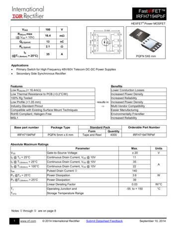
FastIRFET IRFH7194PbFHEXFET Power MOSFETVDSS100VRDS(on) max(@ VGS 10V)16.4m Qg (typical)13nCRg (typical)2.1 ID(@TC (Bottom) 25 C)35APQFN 5X6 mmApplications Primary Switch for High Frequency 48V/60V Telecom DC-DC Power Supplies Secondary Side Synchronous RectifierFeaturesLow RDS(ON) ( 16.4m )Low Thermal Resistance to PCB ( 3.2 C/W)100% Rg TestedLow Profile ( 1.05 mm)Industry-Standard PinoutCompatible with Existing Surface Mount TechniquesRoHS Compliant, Halogen-FreeMSL1Base part numberPackage TypeIRFH7194PbFPQFN 5mm x 6 mmBenefitsLower Conduction LossesIncreased Power DensityIncreased Reliabilityresults in Increased Power DensityMulti-Vendor Compatibility Easier ManufacturingEnvironmentally FriendlierIncreased ReliabilityStandard PackFormQuantityTape and Reel4000Orderable Part NumberIRFH7194TRPbFAbsolute Maximum RatingsMax.UnitsVGSGate-to-Source VoltageParameter 20VID @ TA 25 CContinuous Drain Current, VGS @ 10V11ID @ TC(Bottom) 25 CContinuous Drain Current, VGS @ 10V35ID @ TC(Bottom) 100 CContinuous Drain Current, VGS @ 10V22IDMPulsed Drain Current 140PD @TA 25 CPower Dissipation3.6PD @TC(Bottom) 25 CPower Dissipation39AWLinear Derating Factor0.03W/ CTJOperating Junction and-55 to 150 CTSTGStorage Temperature RangeNotes through are on page 81www.irf.com 2014 International RectifierSubmit Datasheet FeedbackSeptember 10, 2014
IRFH7194PbFStatic @ TJ 25 C (unless otherwise specified)ParameterBVDSSDrain-to-Source Breakdown Voltage BVDSS/ TJ Breakdown Voltage Temp. CoefficientRDS(on)Static Drain-to-Source On-ResistanceVGS(th)Gate Threshold VoltageGate Threshold Voltage Coefficient VGS(th)IDSSDrain-to-Source Leakage CurrentIGSSGate-to-Source Forward LeakageGate-to-Source Reverse LeakagegfsForward TransconductanceQgTotal Gate ChargeQgs1Pre-Vth Gate-to-Source ChargeQgs2Post-Vth Gate-to-Source ChargeQgdGate-to-Drain ChargeQgodrGate Charge OverdriveQswSwitch Charge (Qgs2 Qgd)QossOutput ChargeRGGate Resistancetd(on)Turn-On Delay TimetrRise Timetd(off)Turn-Off Delay TimetfFall TimeCissInput CapacitanceCossOutput CapacitanceCrssReverse Transfer CapacitanceDiode CharacteristicsParameterISContinuous Source Current(Body Diode)ISMPulsed Source Current(Body Diode) VSDDiode Forward VoltagetrrReverse Recovery TimeQrrReverse Recovery ��UnitsVmV/ Cm VmV/ ––140UnitsConditionsAMOSFET symbolshowing theintegral reversep-n junction diode.VTJ 25 C, IS 21A, VGS 0V ns TJ 25 C, IF 21A, VDD 50VnC di/dt 100A/µs SnCnC ConditionsVGS 0V, ID 250µAReference to 25 C, ID 1mAVGS 10V, ID 21A VDS VGS, ID 50µAVDS 80V, VGS 0VVGS 20VVGS -20VVDS 25V, ID 21AVDS 50VVGS 10VID 21AVDS 50V, VGS 0VnsVDD 50V, VGS 10VID 21ARG 1.0 pFVGS 0VVDS 50Vƒ Avalanche CharacteristicsEAS (Thermally limited)ParameterSingle Pulse Avalanche Energy Typ.–––Max.220UnitsmJIARAvalanche Current –––12ATyp.–––Max.3.2Units–––22 C/WThermal ResistanceParameterR JC (Bottom) Junction-to-Case Junction-to-Case R JC (Top)R JAJunction-to-Ambient –––35R JA ( 10s)Junction-to-Ambient –––202www.irf.com 2014 International RectifierSubmit Datasheet FeedbackSeptember 10, 2014
IRFH7194PbF1000 60µs PULSE WIDTHTj 25 CID , D ra in -to -S o u rce C u rre n t (A )ID , D ra in -to -S o u rce C u rre n t (A )100010010VGSTOP115V10V7.0V6.0V3.8V0.15.0V4.5V 60µs PULSE WIDTHTj 150 .0V3.8VBOTTOM0.010.11101000.11V DS , Drain-to-Source Voltage (V)100Fig 2. Typical Output Characteristics10002.0100TJ 150 C10TJ 25 C1V DS 50V 60µs PULSE WIDTH0.12.03.04.05.0ID 21AV GS 10V1.81.6(N o rm a liz e d )R D S (o n ) , D ra in -to -S o u rce O n R e sista n ceID , D ra in -to -S o u rc e C u rre n t (A )10V DS , Drain-to-Source Voltage (V)Fig 1. Typical Output Characteristics1.41.21.00.80.66.0-60-40V GS , Gate-to-Source Voltage (V)V GS 0V,C CCC10000issrssoss C Cgsgd, CdsID 21ASHORTEDgdds CgdC oss10002040608010012014016014f 1 MHZ C0Fig 4. Normalized On-Resistance vs. TemperatureV G S , G a te -to -S o u rce V o lta g e (V )100000-20TJ , Junction Temperature ( C)Fig 3. Typical Transfer CharacteristicsC , C a pa citan ce (p F )3.8V0.1C issC rss10012V DS 80V10V DS 20VV DS 50V864201000.1110100V DS , Drain-to-Source Voltage (V)Fig 5.3www.irf.com481216Q G Total Gate Charge (nC) 2014 International RectifierFig 6. Typical Gate Charge vs. Gate-to-Source VoltageSubmit Datasheet FeedbackSeptember 10, 2014
IRFH7194PbF10001000ID , D ra in -to -S o u rce C u rren t (A )IS D , R e ve r se D r a in C u r r e n t ( A )OPERATION IN THIS AREALIMITED BY R(on)DS100TJ 150 C10TJ 25 C1100100µsec1msec1010msec10.1Tc 25 CTj 150 CSingle PulseV GS 0V0.010.10.20.40.60.81.00.11.2110100V DS , Drain-toSource Voltage (V)V SD , Source-to-Drain Voltage (V)Fig 8. Maximum Safe Operating AreaFig 7. Typical Source-Drain Diode Forward Voltage4.0V G S (th ) G ate th resh o ld V o lta g e (V )40ID , D ra in C u rre n t (A )DC3020103.53.0ID 50µAID 250µA2.5ID 1.0mAID 0TJ , Temperature ( C )TC , CaseTemperature ( C)Fig 9. Maximum Drain Current vs. Case TemperatureFig 10. Threshold Voltage vs. TemperatureT h e rm a l R e sp o n s e ( Zth JC ) C /W10D 0.5010.200.100.050.10.020.010.01Notes:1. Duty Factor D t1/t22. Peak Tj P dm x Zthjc TcSINGLE PULSE( THERMAL RESPONSE )0.0011E-0061E-0050.00010.0010.010.11t 1 , Rectangular Pulse Duration (sec)Fig 11. Maximum Effective Transient Thermal Impedance, Junction-to-Case4www.irf.com 2014 International RectifierSubmit Datasheet FeedbackSeptember 10, 2014
IRFH7194PbF100A va la n ch e C u rre n t (A )Allow ed avalanche Currentpulsew idth, tav, assumingTstart 25 C (Single Pulse)vs avalanche Tj 125 C and101Allow ed avalanche Current vs avalanchepulsew idth, tav, assuming j 25 C andTstart 125 C. (Single 1tav (sec)100060E A S , S in g le P u lse A va lan ch e E ne rgy (m J)R D S (on ), D ra in-to -S o urce O n R e sista n ce (m )Fig 12. Typical Avalanche Current vs. Pulse WidthID 21A504030TJ 125 C2010TJ 25 CD2.9A4.6ABOTTOM12A800600400200002468101214161820V GS, Gate -to -Source Voltage (V)Fig 13. On–Resistance vs. Gate Voltage5ITOPwww.irf.com 2014 International Rectifier255075100125150Starting T J , Junction Temperature ( C)Fig 14. Maximum Avalanche Energy vs. Drain CurrentSubmit Datasheet FeedbackSeptember 10, 2014
IRFH7194PbFFig 15. Peak Diode Recovery dv/dt Test Circuit for N-Channel HEXFET Power MOSFETsV (B R )D S Stp15VLVDSD R IV E RD .U .TRGIA S VD D-A20Vtp0 .0 1 IASFig 16a. Unclamped Inductive Test CircuitFig 17a. Switching Time Test CircuitFig 16b. Unclamped Inductive WaveformsFig 17b. Switching Time WaveformsIdVdsVgsVDDV g s(th )Q g s1 Q g s2Fig 18. Gate Charge Test Circuit6www.irf.com 2014 International RectifierQ gdQ godrFig 19. Gate Charge WaveformSubmit Datasheet FeedbackSeptember 10, 2014
IRFH7194PbFPQFN 5x6 Outline "B" Package DetailsFor more information on board mounting, including footprint and stencil recommendation, please refer to application noteAN-1136: .pdfFor more information on package inspection techniques, please refer to application note /an-1154.pdfPQFN 5x6 Outline "B" Part MarkingINTERNATIONALRECTIFIER LOGODATE CODEASSEMBLYSITE CODE(Per SCOP 200-002)PIN 1IDENTIFIERXXXXXYWWXXXXXXPART NUMBER(“4 or 5 digits”)MARKING CODE(Per Marking Spec)LOT CODE(Eng Mode - Min last 4 digits of EATI#)(Prod Mode - 4 digits of SPN code)Note: For the most current drawing please refer to IR website at http://www.irf.com/package/7www.irf.com 2014 International RectifierSubmit Datasheet FeedbackSeptember 10, 2014
IRFH7194PbFPQFN 5x6 Outline "B" Tape and ReelCLNote: For the most current drawing please refer to IR website at http://www.irf.com/package/Qualifiction Information†Industrial(per JEDEC JESD47F†† guidelines)Qualification LevelMoisture Sensitivity LevelPQFN 5mm x 6mmMSL1(per JEDEC J-STD-020D††)YesRoHS Compliant† Qualification standards can be found at International Rectifier’s web site: http://www.irf.com/product-info/reliability/†† Applicable version of JEDEC standard at the time of product release.Notes: Repetitive rating; pulse width limited by max. junction temperature. Starting TJ 25 C, L 3.0mH, RG 50 , IAS 12A. Pulse width 400µs; duty cycle 2%. R is measured at TJ of approximately 90 C. When mounted on 1 inch square PCB (FR-4). Please refer to AN-994 for more /an-994.pdfIR WORLD HEADQUARTERS: 101 N. Sepulveda Blvd., El Segundo, California 90245, USATo contact International Rectifier, please visit http://www.irf.com/whoto-call/8www.irf.com 2014 International RectifierSubmit Datasheet FeedbackSeptember 10, 2014
Tstart 125 C. (Single Pulse) Allow ed avalanche Current vs avalanche pulsew idth, tav, assuming ' Tj 125 C and Tstart 25 C (Single Pulse) 25 50 75 100 125 150 Starting T J , Junction Temperature ( C) 0 200 400 600 800 1000 E) I D TOP 2.9A 4.6A BOTTOM 12A
