Transcription
ESP-12E WiFi ModuleVersion1.0Disclaimer and Copyright Notice.Information in this document, including URL references, is subject to change without notice.THIS DOCUMENT IS PROVIDED AS IS WITH NO WARRANTIES WHATSOEVER, INCLUDING ANYWARRANTY OF MERCHANTABILITY, NONINFRINGEMENT, FITNESS FOR ANY PARTICULAR PURPOSE, OR ANY WARRANTY OTHERWISE ARISING OUT OF ANY PROPOSAL,SPECIFICATIONOR SAMPLE. All liability, including liability for infringement of any proprietary rights, relating to use of information in thisdocument is disclaimed. No licenses express or implied, by estoppel or otherwise, to any intellectual property rights are granted herein.The WiFi Alliance Member Logo is a trademark of the WiFi Alliance.All trade names, trademarks and registered trademarks mentioned in this document are property of their respective owners, and arehereby acknowledged.Copyright 2015 AI-Thinker team. All rights reserved.NoticeProduct version upgrades or other reasons, possible changes in the contents of this manual. AI-Thinker reserves in the absence of anynotice or indication of the circumstances the right to modify the content of this manual. This manual is used only as a guide, Ai-thinkermake every effort to provide accurate information in this manual, but Ai-thinker does not ensure that manual content without error, inthis manual all statements, information and advice nor does it constitute any express or implied warranty.
Table of Contents1. Preambles . 31.1.Features . 41.2.Parameters . 62. Pin Descriptions . 73. Packaging and Dimension . 94. Functional Descriptions . 114.1.MCU . 114.2.Memory Organization . 114.2.1. Internal SRAM and ROM . 114.2.2. External SPI Flash . 114.3.Crystal . 124.4.Interfaces . 124.5.Absolute Maximum Ratings . 144.6.Recommended Operating Conditions . 144.7.Digital Terminal Characteristics . 145. RF Performance . 156. Power Consumption . 167. Reflow Profile . 178. Schematics . 18
1.PreamblesESP-12E WiFi module is developed by Ai-thinker Team. core processor ESP8266 in smaller sizes of the moduleencapsulates Tensilica L106 integrates industry-leading ultra low power 32-bit MCU micro, with the 16-bit short mode,Clock speed support 80 MHz, 160 MHz, supports the RTOS, integrated Wi-Fi MAC/BB/RF/PA/LNA, on-board antenna.The module supports standard IEEE802.11 b/g/n agreement, complete TCP/IP protocol stack. Users can use theadd modules to an existing device networking, or building a separate network controller.ESP8266 is high integration wireless SOCs, designed for space and power constrained mobile platform designers.It provides unsurpassed ability to embed Wi-Fi capabilities within other systems, or to function as a standaloneapplication, with the lowest cost, and minimal space requirement.Figure 1 ESP8266EX Block DiagramESP8266EX offers a complete and self-contained Wi-Fi networking solution; it can be used to host the applicationor to offload Wi-Fi networking functions from another application processor.When ESP8266EX hosts the application, it boots up directly from an external flash. In has integrated cache toimprove the performance of the system in such applications.Alternately, serving as a Wi-Fi adapter, wireless internet access can be added to any micro controllerbased designwith simple connectivity (SPI/SDIO or I2C/UART interface).ESP8266EX is among the most integrated WiFi chip in the industry; it integrates the antenna switches, RF balun,power amplifier, low noise receive amplifier, filters, power management modules, it requires minimal external circuitry,and the entire solution, including front-end module, is designed to occupy minimal PCB area.Shenzhen Anxinke Technology CO;LTDhttp://www.ai-thinker.com3
ESP8266EX also integrates an enhanced version of Tensilica’s L106 Diamond series 32-bit processor, with on-chipSRAM, besides the Wi-Fi functionalities. ESP8266EX is often integrated with external sensors and other applicationspecific devices through its GPIOs; codes for such applications are provided in examples in the SDK.Espressif Systems’ Smart Connectivity Platform (ESCP) demonstrates sophisticated system-level features includefast sleep/wake context switching for energy-efficient VoIP, adaptive radio biasing. for low-power operation, advancesignal processing, and spur cancellation and radio co-existence features for common cellular, Bluetooth, DDR, LVDS,LCD interference mitigation.1.1.Features 802.11 b/g/n Integrated low power 32-bit MCU Integrated 10-bit ADC Integrated TCP/IP protocol stack Integrated TR switch, balun, LNA, power amplifier and matching network Integrated PLL, regulators, and power management units Supports antenna diversity Wi-Fi 2.4 GHz, support WPA/WPA2 Support STA/AP/STA AP operation modes Support Smart Link Function for both Android and iOS devices Support Smart Link Function for both Android and iOS devices SDIO 2.0, (H) SPI, UART, I2C, I2S, IRDA, PWM, GPIO STBC, 1x1 MIMO, 2x1 MIMO A-MPDU & A-MSDU aggregation and 0.4s guard intervalShenzhen Anxinke Technology CO;LTDhttp://www.ai-thinker.com4
Deep sleep power 10uA, Power down leakage current 5uA Wake up and transmit packets in 2ms Standby power consumption of 1.0mW (DTIM3) 20dBm output power in 802.11b mode Operating temperature range -40C 125CShenzhen Anxinke Technology CO;LTDhttp://www.ai-thinker.com5
1.2.ParametersTable 1 below describes the major parameters.Table 1 ParametersShenzhen Anxinke Technology CO;LTDhttp://www.ai-thinker.com6
2.Pin DescriptionsThere are altogether 22 pin counts, the definitions of which are described in Table 2 below。Table 2 ESP-12E Pin designTable 3 Pin DescriptionsNO.Pin unctionReset the moduleA/D Conversion result.Input voltage range 0-1v,scope:0-1024Chip enable pin.Active highGPIO16; can be used to wake up the chipset from deep sleep mode.GPIO14; HSPI CLKGPIO12; HSPI MISOGPIO13; HSPI MOSI; UART0 CTS3.3V power supply (VDD)Chip selectionSalve output Main inputShenzhen Anxinke Technology CO;LTDhttp://www.ai-thinker.com7
O0IO4IO5RXDTXDGPIO9GBIO10Main output slave inputClockGNDGPIO15; MTDO; HSPICS; UART0 RTSGPIO2; UART1 TXDGPIO0GPIO4GPIO5UART0 RXD; GPIO3UART0 TXD; GPIO1Table 4 Pin ModeModeGPIO15GPIO0GPIO2UARTLowLowHighFlash BootLowHighHighShenzhen Anxinke Technology CO;LTDhttp://www.ai-thinker.com8
Table 5 Receiver Sensitivity3.Packaging and DimensionThe external size of the module is 16mm*24mm*3mm, as is illustrated in Figure 3 below. The type of flash integratedin this module is an SPI flash, the capacity of which is 4 MB, and the package size of which is SOP-210mil. The antennaapplied on this module is a 3DBi PCB-on-board antenna.Shenzhen Anxinke Technology CO;LTDhttp://www.ai-thinker.com9
Figure 3 [Module Pin Counts, 22 pin, 16 mm *24 mm *3 mm]Figure 4 Top View of ESP-12E WiFi ModuleShenzhen Anxinke Technology CO;LTDhttp://www.ai-thinker.com10
Table 5 Dimension of ESP-12E WiFi ModulLengthWidthHeightPAD Size(Bottom)Pin Pitch16 mm24mm3 mm0.9 mm x 1.7 mm2mm4. Functional Descriptions4.1.MCUESP8266EX is embedded with Tensilica L106 32-bit micro controller (MCU), which features extra low powerconsumption and 16-bit RSIC. The CPU clock speed is 80MHz. It can also reach a maximum value of 160MHz.ESP8266EX is often integrated with external sensors and other specific devices through its GPIOs; codes for suchapplications are provided in examples in the SDK.4.2.Memory Organization4.2.1.Internal SRAM and ROMESP8266EX WiFi SoC is embedded with memory controller, including SRAM and ROM. MCU can visit the memoryunits through iBus, dBus, and AHB interfaces. All memory units can be visited upon request, while a memory arbiterwill decide the running sequence according to the time when these requests are received by the processor.According to our current version of SDK provided, SRAM space that is available to users is assigned as below: RAM size 36kB, that is to say, when ESP8266EX is working under the station mode and is connected to therouter, programmable space accessible to user in heap and data section is around 36kB.) There is no programmable ROM in the SoC, therefore, user program must be stored in an external SPI flash.4.2.2.External SPI FlashThis module is mounted with an 4 MB external SPI flash to store user programs. If larger definable storage spaceis required, a SPI flash with larger memory size is preferred. Theoretically speaking, up to 16 MB memory capacity canbe supported.Suggested SPI Flash memory capacity: OTA is disabled: the minimum flash memory that can be supported is 512 kB; OTA is enabled: the minimum flash memory that can be supported is 1 MB.Several SPI modes can be supported, including Standard SPI, Dual SPI, and Quad SPI.Shenzhen Anxinke Technology CO;LTDhttp://www.ai-thinker.com11
Therefore, please choose the correct SPI mode when you are downloading into the flash, otherwisefirmwares/programs that you downloaded may not work in the right way.4.3.CrystalCurrently, the frequency of crystal oscillators supported include 40MHz, 26MHz and 24MHz. The accuracy ofcrystal oscillators applied should be 10PPM, and the operating temperature range should be between -20 C and 85 C.When using the downloading tools, please remember to select the right crystal oscillator type. In circuit design,capacitors C1 and C2, which are connected to the earth, are added to the input and output terminals of the crystaloscillator respectively. The values of the two capacitors can be flexible, ranging from 6pF to 22pF, however, the specificcapacitive values of C1 and C2 depend on further testing and adjustment on the overall performance of the wholecircuit. Normally, the capacitive values of C1 and C2 are within 10pF if the crystal oscillator frequency is 26MHz, whilethe values of C1 and C2 are 10pF C1, C2 22pF if the crystal oscillator frequency is 40MHz.4.4.InterfacesTable 6 Descriptions of InterfacesShenzhen Anxinke Technology CO;LTDhttp://www.ai-thinker.com12
Shenzhen Anxinke Technology CO;LTDhttp://www.ai-thinker.com13
4.5.Absolute Maximum RatingsTable 7 Absolute Maximum Ratings4.6.Recommended Operating ConditionsTable 8 Recommended Operating Conditions4.7.Digital Terminal CharacteristicsTable 9 Digital Terminal CharacteristicsNote: Test conditions: VDD 3.3V, Temperature 20 , if nothing special is stated.Shenzhen Anxinke Technology CO;LTDhttp://www.ai-thinker.com14
5. RF PerformanceTable 10 RF PerformanceShenzhen Anxinke Technology CO;LTDhttp://www.ai-thinker.com15
6. Power ConsumptionTable 11 Power Consumption❶Modem-Sleep requires the CPU to be working, as in PWM or I2S applications. According to 802.11 standards (likeU-APSD), it saves power to shut down the Wi-Fi Modem circuit while maintaining a Wi-Fi connection with no datatransmission. E.g. in DTIM3, to maintain a sleep 300mswake 3ms cycle to receive AP’s Beacon packages, the current isabout 15mA.❷ During Light-Sleep, the CPU may be suspended in applications like Wi-Fi switch. Without data transmission, theWi-Fi Modem circuit can be turned off and CPU suspended to save power according to the 802.11 standard (U-APSD).E.g. in DTIM3, to maintain a sleep 300ms-wake 3ms cycle to receive AP’s Beacon packages, the current is about 0.9mA.❸ Deep-Sleep does not require Wi-Fi connection to be maintained. For application with long time lags between datatransmission, e.g. a temperature sensor that checks the temperature every 100s ,sleep 300s and waking up to connectto the AP (taking about 0.3 1s), the overall average current is less than 1mA.Shenzhen Anxinke Technology CO;LTDhttp://www.ai-thinker.com16
7. Reflow ProfileTable 12 InstructionsShenzhen Anxinke Technology CO;LTDhttp://www.ai-thinker.com17
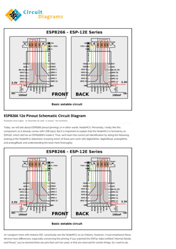
8. SchematicsFigure 4 Schematics of Esp-12E WiFi ModuleShenzhen Anxinke Technology CO;LTDhttp://www.ai-thinker.com18
Shenzhen Anxinke Technology CO;LTD http://www.ai-thinker.com 3 1. Preambles ESP-12E WiFi module is developed