Transcription
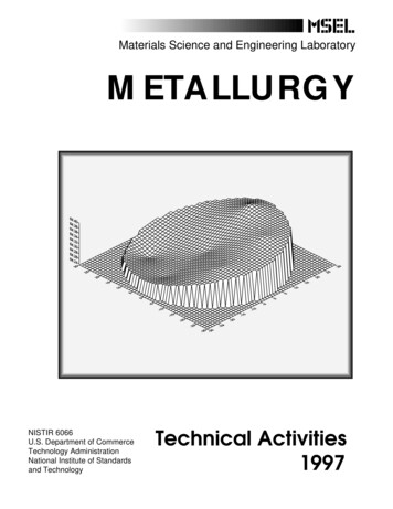
Materials Science and Engineering LaboratoryMETALLURGYNISTIR 6066U.S. Department of CommerceTechnology AdministrationNational Institute of Standardsand TechnologyTechnical Activities1997
Certain companies and commercial products are mentioned in this report. They are used to eithercompletely specify a procedure or describe an interaction with NIST. Such mention is not meant asan endorsement by NIST or to represent the best choice for that purpose.ii
METALLURGY DIVISIONCHIEFCarol A. HandwerkerPhone (301) 975-6158DEPUTY CHIEFRobert J. SchaeferPhone (301) 975-5961GROUP LEADERSElectrochemical ProcessingGery R. StaffordPhone (301) 975-6412Magnetic MaterialsRobert D. ShullPhone (301) 975-6035Materials PerformanceE. Neville PughPhone (301) 975-4679Materials Structure and CharacterizationFrank W. GaylePhone (301) 975-6161Metallurgical ProcessingJohn R. ManningPhone (301) 975-6157iii
TABLE OF CONTENTSPageINTRODUCTION . . . . . . . . . . . . . . . . . . . . . . . . . . . . . . . . . . . . . . . . . . . . . . . . . . . . 1ELECTRONIC PACKAGING, INTERCONNECTION AND ASSEMBLY . . . . . . . . . . . . . 7Lead-Free Solders . . . . . . . . . . . . . . . . . . . . . . . . . . . . . . . . . . . . . . . . . . . . . . 8High-Temperature Solders for Microelectronics . . . . . . . . . . . . . . . . . . . . . . . . . . . 10Solderability Measurements for Microelectronics . . . . . . . . . . . . . . . . . . . . . . . . . . 12Solder Interconnect Design . . . . . . . . . . . . . . . . . . . . . . . . . . . . . . . . . . . . . . . . . 14Stress Measurements in Electronic Packaging . . . . . . . . . . . . . . . . . . . . . . . . . . . . . 16Solder Jet Printing for Microelectronics Applications . . . . . . . . . . . . . . . . . . . . . . . . 18INTELLIGENT PROCESSING OF MATERIALS . . . . . . . . . . . . . . . . . . . . . . . . . . . . . . 21Solidification Path Modeling for Casting of Multicomponent Aerospace Alloys . . . . . . 22Generation of Grain Defects Near Corners and Edges in Castings . . . . . . . . . . . . . . . 24Porosity in Castings . . . . . . . . . . . . . . . . . . . . . . . . . . . . . . . . . . . . . . . . . . . . . 26Thermophysical Data for Castings . . . . . . . . . . . . . . . . . . . . . . . . . . . . . . . . . . . . 29Magnetics for Steel Processing . . . . . . . . . . . . . . . . . . . . . . . . . . . . . . . . . . . . . . 31MAGNETIC MATERIALS . . . . . . . . . . . . . . . . . . . . . . . . . . . . . . . . . . . . . . . . . . . . . . 33Giant Magnetoresistance Materials . . . . . . . . . . . . . . . . . . . . . . . . . . . . . . . . . . . . 34Processing and Micromagnetics of Thin Magnetic Films . . . . . . . . . . . . . . . . . . . . . 39Magnetic Properties of Nanomaterials . . . . . . . . . . . . . . . . . . . . . . . . . . . . . . . . . . 42METALS DATA AND CHARACTERIZATION . . . . . . . . . . . . . . . . . . . . . . . . . . . . . . . . 47Thermophysical Properties . . . . . . . . . . . . . . . . . . . . . . . . . . . . . . . . . . . . . . . . . 48Microstructural Studies of Complex Phases . . . . . . . . . . . . . . . . . . . . . . . . . . . . . . 51Mechanical and Thermal Properties of Multilayered Materials . . . . . . . . . . . . . . . . . . 54Hardness Standards . . . . . . . . . . . . . . . . . . . . . . . . . . . . . . . . . . . . . . . . . . . . . . 58Magnetic Properties and Standard Reference Materials . . . . . . . . . . . . . . . . . . . . . . . 62Lightweight Materials for Automotive Applications . . . . . . . . . . . . . . . . . . . . . . . . . 63Performance of Structural Materials . . . . . . . . . . . . . . . . . . . . . . . . . . . . . . . . . . . 68Performance of Materials in Corrosive Media . . . . . . . . . . . . . . . . . . . . . . . . . . . . . 73Magneto-Optical Imaging . . . . . . . . . . . . . . . . . . . . . . . . . . . . . . . . . . . . . . . . . . 77Development of Scanning Acoustic Microscopy . . . . . . . . . . . . . . . . . . . . . . . . . . . 79Electron Microscopy . . . . . . . . . . . . . . . . . . . . . . . . . . . . . . . . . . . . . . . . . . . . . 81METALS PROCESSING . . . . . . . . . . . . . . . . . . . . . . . . . . . . . . . . . . . . . . . . . . . . . . . 84Processing of Advanced Materials . . . . . . . . . . . . . . . . . . . . . . . . . . . . . . . . . . . . 85Solidification Modeling . . . . . . . . . . . . . . . . . . . . . . . . . . . . . . . . . . . . . . . . . . . 88iv
Sensors and Diagnostics for Thermal Spray Processes . . . . . . . . . . . . . . . . . . . . . . . 91Electrodeposition of Alumium Alloys . . . . . . . . . . . . . . . . . . . . . . . . . . . . . . . . . . 94Electrodeposited Coating Thickness Standards . . . . . . . . . . . . . . . . . . . . . . . . . . . . 97Gold Microhardness Standards . . . . . . . . . . . . . . . . . . . . . . . . . . . . . . . . . . . . . . 98Electrogalvanzied Coatings on Steel . . . . . . . . . . . . . . . . . . . . . . . . . . . . . . . . . . . 99Electrodeposited Chromium from Trivalent Electrolytes . . . . . . . . . . . . . . . . . . . . . 100Electrochemical Processing of Nanoscale Materials . . . . . . . . . . . . . . . . . . . . . . . . 102DENTAL AND MEDICAL MATERIALS . . . . . . . . . . . . . . . . . . . . . . . . . . . . . . . . . . . 106Advanced Restorative Dental Materials . . . . . . . . . . . . . . . . . . . . . . . . . . . . . . . . 107EVALUATED MATERIALS DATA . . . . . . . . . . . . . . . . . . . . . . . . . . . . . . . . . . . . . . . 110NACE-NIST Corrosion Data Program . . . . . . . . . . . . . . . . . . . . . . . . . . . . . . . . 111HIGH TEMPERATURE SUPERCONDUCTIVITY . . . . . . . . . . . . . . . . . . . . . . . . . . . . 113Magnetic Properties of Superconductors . . . . . . . . . . . . . . . . . . . . . . . . . . . . . . . 114ADDITIONAL OUTPUT . . . . . . . . . . . . . . . . . . . . . . . . . . . . . . . . . . . . . . . . . . . . . . 116RESEARCH STAFF . . . . . . . . . . . . . . . . . . . . . . . . . . . . . . . . . . . . . . . . . . . . . . . . . 117ORGANIZATIONAL CHARTS . . . . . . . . . . . . . . . . . . . . . . . . . . . . . . . . . . . . . . . . . . .Metallurgy Division . . . . . . . . . . . . . . . . . . . . . . . . . . . . . . . . . . . . . . . . . . . . . 123Materials Science and Engineering . . . . . . . . . . . . . . . . . . . . . . . . . . . . . . . . . . . 124National Institute of Standards & Technology . . . . . . . . . . . . . . . . . . . . . . . . . . . 125v
INTRODUCTIONCarol A. Handwerker, ChiefThis report describes the major technical activities and accomplishments of the MetallurgyDivision in 1997, and, therefore, reflects the research priorities established after extensiveconsultation and collaboration with our customers in US industry. It also reflects the Programplanning and management structure that we have developed within the Materials Science andEngineering Laboratory (MSEL) to meet the identified needs of the Nation’s measurement andstandards infrastructure. The Division is organized administratively into groups that represent theDivision’s core expertise in Metallurgical Processing, Electrochemical Processing, MagneticMaterials, Materials Structure and Characterization, and Materials Performance. However, byvirtue of the interdisciplinary nature of materials science and engineering, the Program teams cutacross the Division’s management groups and, in many cases, cut across MSEL Divisions and theNIST Laboratories in order to best meet the scientific and technical needs of our customers. Wehope that this report provides insight into how our research programs meet the objectives of ourcustomers, how the capabilities of the Metallurgy Division are being used to solve problemsimportant to the national economy and the measurements and standards infrastructure, and how weinteract with our customers to establish new priorities and programs. We welcome advice andsuggestions from our customers on how we can better serve their needs.The NIST Metallurgy Division mission is to provide measurement methods, standards, anda fundamental understanding of materials behavior to aid US industry in the more effectiveproduction and use of both traditional and emerging materials. As part of this mission we areresponsible not only for developing new measurement methodologies with broad applicabilityacross materials classes and industries, but also for working with individual industry groups todevelop and integrate measurements, standards, and evaluated data for specific, technologicallyimportant applications.The Metallurgy Division philosophy is that the development of measurement methods mustbe coupled with a fundamental understanding of the relationship among materials structure,processing, and properties in order to have a lasting impact in measurement science and theindustries we serve. Two examples of this philosophy are: Beginning in 1990, NIST set up a major new research program specifically aimed atproviding the scientific understanding and measurement capability needed to enable U.S.industry to make the best GMR materials in the world. This program was centered on anew facility, known as the Magnetic Engineering Research Facility (MERF), which is oneof the most advanced magnetic thin-film production plants ever constructed. From thebeginning, NIST researchers have developed the measurement techniques, clarified thescientific issues, and established the manufacturing processes needed to produce thehighest quality GMR materials. Once again this year, research at MERF is defining thestate-of-the-art in magnetic thin film fabrication. NIST researchers at MERF set a newrecord for the largest value ever recorded in the type of material (a spin valve with one Culayer) best suited to commercial products, discovered that increasing specular electron1
scattering at the top and bottom surfaces of a spin valve plays a key role in achieving thelargest possible GMR values, and found two processing methods for increasing specularelectron scattering. These NIST discoveries were transferred to U.S. industry as quicklyas possible for implementation in its manufacturing facilities. Thermal barrier coatings protect engine parts from the elevated temperatures of thecombustion process. It had been proposed that the presence of the numerous interfaces inmultilayer thermal barrier coatings decreases their thermal conductivity, making multilayercoatings more effective thermal barriers than the materials from which they aremanufactured. High-temperature measurements using NIST's pulsed laser heating systemestablished that the upper bound for the interface thermal resistance in industry-suppliedcoatings is orders of magnitude below the postulated value driving industrial multilayerthermal barrier coatings research. An industrial consortium will decide by the end of 1997,based, in part, on these measurements, whether to continue its program on multilayerthermal barrier coatings for engine applications.In 1997, outstanding achievements by Metallurgy Division staff to measurement scienceand technology transfer were recognized in the areas of high-temperature thermophysics andnational hardness standards. Ared Cezairlian was awarded the Yeram S. Touloukian Award of theAmerican Society of Mechanical Engineers (June 1997) in recognition of his novel systems for thehigh-speed, high precision measurement of thermophysical properties of materials at hightemperatures. His recent designs of computer-controlled high-speed optical techniques allowedmeasurement of thermal and related properties at high temperatures for complex alloys important tothe aerospace industry. Sam Low and David Pitchure of the Metallurgy Division, Walter Liggett ofthe Information Technology Laboratory, and Jun Feng Song and Ted Vorburger of theManufacturing Engineering Laboratory were awarded the NIST Rosa Award in recognition of theirdevelopment and the international acceptance of their method for the more accurate determination ofthe Rockwell C Hardness, a measured materials property of great importance in manufacturing andcommerce. Sam Low’s leadership of this NIST program and of the American delegation to ISO9000 hardness committee has been critical to the establishment of a new dimensional-metrologybased approach to the measurement of hardness.The Division uses most of its resources to meet specific, high priority measurement-relatedneeds identified by the aerospace, automotive, magnetic recording, microelectronics, and stationarypower generation industries. Industrial priorities were established through formal and informalmeans: industrial roadmapping activities, workshops, technical meetings, standards committeeparticipation, and individual visits with our customers. In order for us to undertake a new programor project within an existing program, several criteria must be met: (1) there must be a clearresearch need; (2) the NIST role must be consistent with the NIST and Metallurgy Divisionmissions; (3) the industrial and NIST resources must be sufficient to accomplish the goals; and (4)there must be a clear path for technology transfer of NIST results, whether the results are afundamental understanding of materials behavior, measurement techniques, standards, evaluateddata, software, or sensors. The list of research accomplishments that follows provides anindication of the scope and quality of programs in the Metallurgy Division.2
METALLURGY DIVISIONSIGNIFICANT ACCOMPLISHMENTS AND IMPACTElectronic Packaging, Interconnection and Assembly Solder Interconnect Design for Microelectronics - The Solder Interconnect DesignTeam, organized by the Metallurgy Division and the NIST Center for Theoretical andComputational Materials Science, is developing software that will facilitate the design ofelectronic packaging. The Design Team, which includes Motorola, DEC, Ford,Susquehanna University, and others, has used this software to determine equilibriumshapes of solder joints and resulting forces on the electronic package leads. Industrialapplication of the software is spreading rapidly. At Motorola, the software has allowedelectronic packaging engineers to redesign circuit boards in production; as a result of thecalculations, component "fall off" while soldering the second side of a two-sidedproduction circuit board was virtually eliminated, changing the manufacturing yield from20 percent to over 90 percent. In another soldering challenge, a product suffered from"floating and twisting" of every battery contact during soldering, requiring each contact tobe repositioned by hand, a serious manufacturing failure. Using the software and insightsgained at the semi-annual NIST Solder Interconnect Design Team meetings, Motorolasolved this problem as well. High Temperature Fatigue-Resistant Solder Alloys - NIST has taken a leadershiprole in the NCMS Consortium for the Development of High Temperature Fatigue-ResistantSolders, whose members include Delco Electronics, Ford Motor Company, AlliedSignal,Indium Corporation of America, Heraeus Cermalloy, Johnson Manufacturing, AmesLaboratory , and Rensselaer Polytechnic Institute. NIST’s role is to provide a fundamentalknowledge of materials processing and the physical metallurgy of solder joint formation.In FY 1997, NIST, in collaboration with Indium Corporation, discovered a new class ofalloys with promising wetting characteristics and thermal fatigue behavior; these alloyswere the subject of a patent disclosure by NIST and Indium Corporation. Measurements of Residual Stresses in Electronic Packaging - Measurements ofresidual stresses in chip packages using a scanning acoustic microscopy techniquedeveloped at NIST demonstrated that significant levels of residual stresses remain evenafter delamination has occurred between the chip and the mold compound. The acousticmicroscope measurements, performed in collaboration with Texas Instruments,demonstrated that these residual stresses can be detected over a wide frequency range (15150 MHZ). It was also shown that the observed gradual phase shift is frequencyindependent in agreement with the model for scanning acoustic imaging of stress.3
Intelligent Processing of Materials Solidification Path Modeling in Multicomponent Aerospace Alloys - TheNIST software for computation of enthalpy-temperature relationships appropriate formulticomponent alloy solidification has been incorporated into ProCASTTM, a commercialsoftware code, as part of the NIST Consortium on Casting of Aerospace Alloys. Such datawill be used by the investment casting industry to shorten design cycles for production ofturbine engine parts. Modeling Grain Nucleation in Superalloy Castings - Single crystal superalloycastings enable aircraft turbine engines and, more recently, industrial gas turbines, tooperate at higher temperatures and thus at higher efficiencies. Defects such as stray grainsor regions of crystallographic misalignment degrade the high-temperature performance ofsuperalloys and thus cause a high reject rate in these castings. NIST scientists havedeveloped a method to predict when conditions in the casting will be favorable for spuriousgrain nucleation. This time-efficient computational method incorporates thermal simulationresults and the anisotropic growth kinetics of a dendritic front to compute the completetime-temperature history of a three-dimensional casting and time-minimized path to anygiven location in the casting. Experimental nucleation data or an analytical nucleation rateexpression can then be used to quantify the nucleation tendency along the path. Thismethod is being linked to ProCASTTM.Magnetic Materials Measurements of the Thermal Stability of Spin Valves - A method has beendeveloped for characterizing the reversible and irreversible temperature dependence of spinvalve magnetoresistance that involves measurement of magnetoresistance (R vs. appliedfield) at increasingly elevated temperatures and at room temperature following each heating.The measurements at high T reflect both reversible and irreversible changes, while theroom T measurements reflect only irreversible changes as a function of annealingtemperature. Thermal Stability of Spin Valves Improved - The thermal stability of thin magneticfilm spin valves with the highest value of giant magnetoresistance (GMR) ever recordedhas been improved from 250 C to 325 C by adding a 5 nm thick capping layer of tantalum.This 75 C improvement is particularly significant since lithographic practices used in circuitconstruction (including these devices) generally use photoresists which need baking attemperatures close to 250 C.4
Metals Data and Characterization International Hardness Intercomparison - As a result of NIST development ofnational hardness standards, agreement on international hardness scales is developing. Anintercomparison study using the new NIST Rockwell C Scale SRM test blocks, conductedby NIST and the National Research Laboratory of Metrology in Japan, showed agreementwithin /- 0.1 HRC at all three levels of hardness for which the NIST standards areproduced. An intercomparison of the HRB scale was also conducted with Japan andagreement to /- 0.15 HRB was found at four levels of hardness. This unprecedentedagreement is a direct result of NIST research in identifying and quantifying the individualuncertainties associated with the variability of diamond indentors, the standard test blocks,the load cycle, and the testing machine. New Corrosion Test Method Supports Alloy Development - Crucible MaterialsCorporation is developing new corrosion-resistant high nitrogen stainless steels producedby gas atomization and HIP consolidation, with sponsorship from the AdvancedTechnology Program and through a CRADA with the NIST Metallurgy Division. Sinceexisting corrosion test methods were unable to induce pitting corrosion of these highlyresistant alloys, differences in the corrosion resistance of these alloys could not bemeasured. A new pitting corrosion test technique that employs more aggressive conditionswas developed at NIST. The technique has been adopted by Crucible to support their alloydevelopment program. New Measurement Methods for Fundamental Studies of Formability - NISTis working with ATP awardees in the automobile industry to develop constitutive modelsfor metal deformation which can be used in modeling sheet metal formability. Usingneutron scattering and synchrotron X-ray measurements, combined with analyses of X-rayand neutron scattering by dislocations, the NIST work is leading to methods for thedetermination of dislocation content and arrangement in bulk samples of materials. Thisinformation is needed to predict the changes in deformation behavior which developcontinuously during the forming process. High-Speed Laser Polarimeter is Commercialized - The high-speed (millisecondresolution) laser polarimeter, developed jointly by NIST and Containerless ResearchIncorporated (CRI) to enhance the NIST facilities for measurement of fundamentalthermophysical properties, has been commercialized by CRI and has been successfullymarketed internationally. This innovative instrument will significantly simplify the accuratemeasurement of high temperatures by directly determining the normal spectral emissivity ofa specimen surface without the requirement of a blackbody configuration.5
Metals Processing Materials Processing for Non-linear Optical Materials - Bunching of theelementary steps during layerwise growth of crystals for optical applications causesimpurity segregation, inhomogeneous optical properties, and decreased damage thresholdsin the crystals. Analytic and numerical calculations have been used to determine the fluidflow conditions required to avoid step bunching during crystal growth of KDP, largecrystals of which are required for laser fusion applications. Realistic modeling of thegrowth process required extension of a previous theory to include nonlinear anisotropicinterface kinetics. In addition, optimized growth conditions identified in the NIST researchcan now be used to produce higher quality lead bromide-silver bromide crystals asnon-linear optical materials. Imaging Pyrometer for Spray/Atomization Processes - NIST/SBIR-fundedresearch has resulted in a new imaging pyrometer with wide applicability to materialsatomization processing. This “Thermal Spray Imaging” sensor, developed by Stratonics,Inc. of Laguna Hills, CA, uses special IR optics to produce a high resolution two-colorimage of the material under test. This approach provides both temperature and emissivitydata with spatial resolution as high as 15 µm. Equipped with a standard video CCD array,this device can measure real-time accurate surface temperatures ( 10 K), emissivity, androughness of such objects as plasma spray coatings, spray deposition substrates, and thesurface of hot or molten materials. An image intensifying camera is currently underdevelopment that will provide similar results from thermal spray and atomization droplets inflight. Gold Microhardness Standard - A 24K gold, low load microhardness standardprototype has now been developed. The surface area is 2.25 cm2 and the deposit thicknessis 200 µm. At a load of 25 grams, more than 1,000 indentations can be made on itssurface. The average Knoop hardness is 75.5 /- 10%. The request for this standard hascome mainly from the electronics industry where gold is electrodeposited on printed circuitboards. Also, the general plating industry for precious metals has requested the standardfor process control of addition agents to Au electrolytes. This microhardness standard isexpected to fill a void in the low hardness, low load SRMs presently offered.Dental and Medical Applications Consolidation of Mercury-Free Dental Restoratives -The American DentalAssociation has obtained an exclusive license for a NIST patent on silver-based fillingmaterials. The patent resulted from developmental work at NIST supported by the NationalInstitute of Dental Research to find an alternative to mercury-containing dental restorativesand a technique to place or consolidate the restorative using normal dental hand tools.6
TECHNICAL ACTIVITIESELECTRONIC PACKAGING, INTERCONNECTION, ANDASSEMBLYToday’s U.S. microelectronics and supporting infrastructure industries are in fierce internationalcompetition to design and produce new smaller, lighter, faster, more functional electronicsproducts more quickly and economically than ever before.In 1994 the NIST Materials Science and Engineering Laboratory (MSEL) began working veryclosely with the U.S. semiconductor packaging, electronic interconnection, assembly, andmaterials supply industries. These effort led to the development of an interdivisional MSELprogram committed to addressing industry’s most pressing materials measurement and standardsissues. These issues are central to the development and utilization of advanced materials andmaterial processes for new product technologies, as outlined in leading industry roadmaps1 . Thevision that accompanies this program - to be the key resource within the Federal Government formaterials metrology development for commercial microelectronics manufacturing - will be realizedthrough the following objectives: develop and deliver standard measurements and data develop and apply in situ measurements on materials and material assemblies havingmicrometer- and submicrometer-scale dimensions quantify and record the divergence of material properties from their bulk values asdimensions are reduced and interfaces are approached develop fundamental understanding of materials needed for future packaging,interconnection and assembly schemesWith these objectives in mind, the program presently consists of nearly twenty separate projectsthat examine key materials-related issues, such as: electrical, thermal, and mechanicalcharacteristics of metal and polymer thin films; solders, solderability and solder joint design2 ;interfaces and adhesion; electromigration and stress voidage; and built up stress and moisture inplastic packages. These projects are always conducted in concert with partners from industrialconsortia, individual companies, academia, and other government agencies. The program isstrongly coupled with other microelectronics programs within government and industry, includingthe National Semiconductor Metrology Program (NSMP)2 . The NSMP is a national resourceresponsible for the development and dissemination of new semiconductor measurementtechnology.More information about this program, and other NIST activities in electronic packaging,7
interconnection and assembly, is contained in Electronics Packaging, Interconnection andAssembly at NIST: Guide and Resources, nts.htm). Copies may be obtained by contactingMichael Schen at (301) 975-6741 or 1 National Technology Roadmap for Semiconductors, Semiconductor Industry Association, SanJose, CA, 1994, 1997 (in draft); National Technology Roadmap for Electronic Interconnections,Institute for Interconnecting and Packaging Electronic Circuits, Lincolnwood, IL, 1995, 1997 (indraft); National Electronics Manufacturing Technology Roadmap, National ElectronicsManufacturing Initiative, Inc., Herndon, VA, 1996.2 http://www.ctcms.nist.gov/programs/solder3 http://www.eeel.nist.gov/810.01/index.htmlProject Title: LEAD-FREE SOLDERSInvestigators: C. A. Handwerker, U. R. Kattner, W. J. Boettinger, J. R. Manning, F. W.Gayle, M. E. Williams, L. Smith, and J. AdamsObjectives:The objectives of this program are to develop environmentally friendly solders asreplacements for tin-lead near-eutectic alloys, the workhorses of the microelectronics industry, andto evaluate the impact of such solders on industrial practice.Technical Description:Scientists from NIST, working with a broad-based industrial consortium organized throughthe National Center for Manufacturing Sciences (NCMS), have established critical tests andprovided materials property data to evaluate Pb-free solder alloys with respect to a wide range ofmanufacturing, performance, and environmental standards.NIST and NCMS had a multi-year CRADA ending in FY97 describing NIST participation inthis 11M research and development program, which is supported almost entirely by in-kindcontributions from each of its members. In addition to NIST, members include AT&T/LucentTechnologies, Rockwell, Texas Instruments, Ford, GM-Hughes, GM-Delco, HamiltonStandard/United Technologies Research Center, Rensselaer Polytechnic Institute, and SandiaNational Laboratories. NIST contributions to this industry-led program included phase diagramdeterminations, materials fabrication, and test development for manufacturing performance andmechanical failure assessments.The project was successfully completed this year, resulting in a comprehensive report.Planned Outcome:Lead-free solder alloys will be evaluated for their potential to replace Sn-Pb eutectic alloys forvarious applications. Guidelines for testing alloys for use in microelectronics interconnects8
will be provided. At the end of the NCMS project, the data will be made publicly available.External Collaborations:Throughout this project, NIST staff have worked closely with the members of the NCMSLead-Free Solder Project, including AT&T, Rockwell, Delco Electronics, Ford Motor Company,Texas Instruments, GM-Hughes, Hamilton Standard/United Technologies Research Center, aswell as with Sandia National Laboratories, Ames Laboratory, and Rensselaer Polytechnic Institute.Accomplishments:In FY 1997 the Metallurgy Division took the responsibility for leading the team in criticallyanalyzing the data, incorporating the results into a final report, and recommending applications forthe candidate solders.Impact:The final report has been written and made publicly available through NCMS. Replacementshave been identified for various applications, particularly for surface mount technology, althoughthere is no universal drop-in replacement for Pb-Sn eu
INTRODUCTION Carol A. Handwerker, Chief This report describes the major technical activities and accomplishments of the Metallurgy Division in 1997, and, therefore, reflects the research priorities established after extensive consultation and collaboration with o
