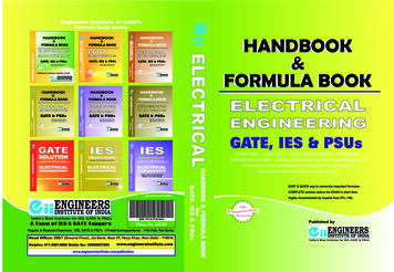
Transcription
GATE, IES & PSUsGATE, IES & PSUsGATE, IES & PSUs9789351377542
FORMULA BOOKforGATE, IES & PSU’sELECTRICALENGINEERINGPublished by Engineers Institute of India
2016 By Engineers Institute of IndiaALL RIGHTS RESERVED. No part of this work covered by the copyrightherein may be reproduced, transmitted, stored or used in any form or by anymeans graphic, electronic, or mechanical & chemical, including but notlimited to photocopying, recording, scanning, digitizing, taping, Webdistribution, information networks, or information storage and retrievalsystems.Engineers Institute of India28-B/7, Jia Sarai, Near IIT Hauz Khas New Delhi-110016Tel: 011-26514888For publication information, visit www.engineersinstitute.com/publicationISBN: 978-93-5156-854-4Price: Rs. 349/-
A WORDWORD TOTO THETHE STUDENTS.AGATE andand EngineeringEngineering Services Examinations are theGATEmost prestigiousprestigious competitivecompetitive examinations conductedmostfor graduategraduate engineers.engineers. Over the past few years, theyforhave becomebecome moremore competitivecompetitive as more and morehavenumbers ofof aspirantsaspirants are increasingly becomingnumbersinterested inin postpost graduate qualifications &interestedgovernment jobsjobs forfor aa securedsecured and bright career.governmentThis FormulaFormula BookBook consistsconsists ofof well-illustratedwell-illustrated concepts, importantThisformulae andand diagrams,diagrams, whichwhich willwill bebe highlyhighly beneficial at the last leg offormulaecandidate’s preparation.preparation.candidate’sincludes allall thethe subjectssubjects ofof ElectricalElectrical Engineering, InstrumentationItIt includesEngineering, whichwhich areare requiredrequired forfor all type of competitiveEngineering,examinations. AdequateAdequate emphasisemphasis hashas beenbeen laid down to all the majorexaminations.topics inin thethe formform ofof TipsTips // Notes,Notes, whichwhich will be highly lucrative fortopicsobjective andand shortshort answeranswer typetype questions.questions.objectiveProper strategystrategy andand revisionrevision isis aa mandatorymandatory requirement for clearingProperany competitivecompetitive examination.examination. ThisThis bookbook covers short notes andanyformulae forfor ElectronicsElectronics && CommunicationCommunication Engineering. This book willformulaehelp inin quickquick revisionrevision beforebefore thethe GATE,GATE, IESIES & all other PSUs.helpWith bestbest wisheswishes forfor futurefuture careercareerWithR. K.K. RajeshRajeshR.DirectorDirectorEngineers InstituteInstitute ofof esh@gmail.com
This book is dedicated to allElectrical EngineersPreparing for GATE, IES, SSC& Public sectorexaminations.
CONTENTS1.NETWORK THEORY . 01-402.CONTROL SYSTEMS . 41-743.DIGITAL ELECTRONICS AND CIRCUITS . 75-1184.MICROPROCESSORS .119-1365.ELECTRONIC DEVICES & CIRCUITS .137-1686.ANALOG ELECTRONICS .169-2047.SIGNALS AND SYSTEMS .205-2308.COMMUNICATION SYSTEMS .231-2649.ELECTROMAGNETIC THEORY .265-28610. MEASUREMENTS AND INSTRUMENTATION .287-30811. ELECTRICAL MACHINES .309-39212. POWER SYSTEMS .393-44813. POWER ELECTRONICS .449-50014. ELECTRICAL MATERIALS .501-514
Why IES?Indian engineering services (IES) constitute of engineers that work under thegovt. of India to manage a large segment of public sector economy whichconstitutes of Railroads, Public works, Power, Telecommunications, etc. IESremain the most sought-after careers for the engineering graduates in India. Acombined competitive examination is conducted by UPSC for recruitment tothe Indian Engineering Services. The exam constitutes of a written examfollowed by an interview for personality test.Why GATE?In the present competitive scenario, where there is mushrooming ofuniversities and engineering colleges, the only yardstick to measureand testthe calibre of engineering students is the GATE.The GATE AdvantageMany public sector undertakings such as BHEL, IOCL, NTPC, BPCL, HPCL, BARCand many more PSUs are using the GATE score for selecting candidates fortheir organizations. Students who qualify in GATE are entitled to a stipend ofRs 8,000 per month during their M.Tech. course. Better remuneration is beingoffered for students of M.Tech./ME as compared to those pursuing B.Tech/B.E.A good rank assures a good job. After joining M.Tech. at IITs and IISc, one canlook at a salary package ranging from Rs 7lakh to 30lakh per annum dependingupon specialization and performance. Clearing GATE is also an eligibility clausefor the award of JRF in CSIR Laboratories.Proper strategy and revision is a mandatory requirement for clearing anycompetitive examination. This book covers short notes and formulae forElectronics & Communication Engineering. This book will help in quickrevision before the GATE, IES & all other PSUs.
EE FORMULA BOOK[1]1. NETWORK THEORY1NETWORK THEORYCONTENTS1.NETWORK BASICS . 02-052.METHODS OF ANALYSIS AND THEOREMS . 06-103.AC FUNDAMENTALS AND R, L, C CIRCUITS .4.RESONANCE . 16-185.TRANSIENTS 6.GRAPH THEORY . 23-267.TWO PORT NETWORKS .27-308.MAGNETIC COUPLED CIRCUITS .31-329.FILTERS .33-3610.NETWORK SYNTHESIS .37-40Published by: ENGINEERS INSTITUTE OF INDIA. ALL RIGHTS RESERVED11-1519-22www.engineersinstitute.com
EE FORMULA BOOK[2]1. NETWORK THEORY1. NETWORK BASICSCurrent: Electric current is the time rate of change of charge flow.dq(Ampere)i dttCharge transferred between time to and tq idttoSign Convention: A negative current of –5A flowing in one direction is same as acurrent of 5A in opposite direction.Voltage: Voltage or potential difference is the energy required to move a unitcharge through an element, measured in volts.Power: It is time rate of expending or absorbing energy. Law of conservation of energy must be obeyed in any electric circuit.Algebraic sum of power in a circuit, at any instant of time, must be zero.i.e. P 0Circuit Elements:Resistor: Linear and bilateral (conduct from both direction)In time domain V(t) I(t)RIn s domainV(s) RI(s)R ρlohmAl length of conductor, resistivity, A area of cross section Extension of wire to n times results in increase in resistance:Published by: ENGINEERS INSTITUTE OF INDIA. ALL RIGHTS RESERVEDR ' n2Rwww.engineersinstitute.com
EE FORMULA BOOK[3]1. NETWORK THEORYR' Compression of wire results in decrease in resistance:Rn2Capacitor: All capacitors are linear and bilateral, except electrolytic capacitorwhich is unilateral.Time Domain:t1v(t) i(t)dtC Cdv(t)i(t) dt1I(s)sC Capacitor doesn’t allow sudden change of voltage, until impulse of current isapplied. It stores energy in the form of electric field and power dissipation in idealcapacitor is zero.1; Xc Capacitive reactance ; 2 f Impedance Zc -jXc & Xc ωCInductor: Linear and Bilateral elementIn s-domain:I(s) sCV(s)V(s) Time Domain:di (t )v(t ) Ldt1i (t ) v(t )dtL ImpedanceZ L jX L tXL &L 1V(s)sL Inductor doesn’t allowed sudden change of current, until impulse of voltage isapplied. It stores energy in the form of magnetic field. Power dissipation in ideal inductor is zero.In s-domainI(s) V(s) sL I(s)Transformer: 4 terminal or 2-port devices.I1I2 Inputport V1 N1OutputV2 portN2–N1 N 2 : Step down transformerV1 N1 V2 N 2Where–N 2 N1 : Step up transformerI1 N 2 I 2 N1N1 K Turns ratio.N2Published by: ENGINEERS INSTITUTE OF INDIA. ALL RIGHTS RESERVEDwww.engineersinstitute.com
EE FORMULA BOOK[4]1. NETWORK THEORYTransformer doesn’t work as amplifier because current decreases in same amountpower remain constant.Gyrator:I1RoV1I2V2R o Coefficient of GyratorV1 R o I 2V2 R o I1 If load is capacitive then input impedance will be inductive and vice versa. If load is inductive then input impedance will be capacitive. It is used for simulation of equivalent value of inductance.Voltage Source:In practical voltage source, there is small internal resistance, so voltage across theelement varies with respect to current. Ideal voltmeter, RV (Internal resistance)Current Source:In practical current source, there is small internal resistance, so current varies withrespect to the voltage across element.Published by: ENGINEERS INSTITUTE OF INDIA. ALL RIGHTS RESERVEDwww.engineersinstitute.com
EE FORMULA BOOK[5]1. NETWORK THEORY Ideal Ammeter, Ra 0 (Internal resistance)Dependent and Independent Source:Independent Source: Voltage or current source whose values doesn’t depend onany other parameters. E.g. Generator etc.Dependent Source: Voltage or current source whose values depend upon otherparameters like current, voltage.The handling of independent and dependent voltage source is identical except.(i) In Thevenin and Norton Theorem(ii) Superposition TheoremWhere, (i) All independent voltage sources are short circuited.(ii) All independent current sources are open circuited.(iii) All dependent voltage and current sources are left as they are. A network in which all network elements are physically separable is known aslumped network. A network in which the circuit elements like resistance, inductance etc, are notphysically separate for analysis purpose, is called distributed network. E.g.Transmission line. If an element is capable of delivering energy independently, then it is calledactive element.Example: Voltage source, Current source If it is not capable of delivering energy, then it is passive element.Example: Resistor, Inductor, Capacitor If voltage and current across an element are related to each other through aconstant coefficient then the element is called as linear element otherwise it iscalled as non-linear. When elements characteristics are independent of direction of current thenelement is called bi-directional element otherwise it is called as unidirectional.Ex: R, L & C. Diode is a unidirectional element. Voltage and current sources are also unidirectional elements. Every linear element should obey the bi-directional property but vice versa as isnot necessary. Internal resistance of voltage source is in series with the source. Internalresistance of ideal voltage source is zero. Internal resistance of current source is in parellel with the source. Internalresistance of ideal current source is infinite.Published by: ENGINEERS INSTITUTE OF INDIA. ALL RIGHTS RESERVEDwww.engineersinstitute.com
EE FORMULA BOOK[6]1. NETWORK THEORY2. METHODS OF ANALYSIS AND THEOREMS(i) Kirchoff’s Points Law or Current Law (KCL): In any electrical network, thealgebric sum of the currents meeting at point (or junction) is zero.Incoming current Outgoing currentI1 I2 I3 I4It is based on conservation of charge.(ii) Kirchoff’s Mesh Law or Voltage Law (KVL): The algebraic sum of productsof currents and resistance in each of conductor in any closed path in a network plusthe algebraic sum of emf in that path is zero.i.e. IR emf 0It is based on conservation of energy.Determination of Voltage Sign(a) Sign of Battery E.M.F.:(b) Sign of IR Drop:Resistors in Series:R eq R1 R 2 R 3 . R nResistors in Parallel:11111 . R eq R1 R 2 R 3RnInductors in Series:Leq L1 L2 L3 . LnInductors in Parallel:11111 . Leq L1 L 2 L3LnCapacitors in Series:11111 . Ceq C1 C2 C3CnCapacitor in Parallel:Ceq C1 C 2 C3 . C nPublished by: ENGINEERS INSTITUTE OF INDIA. ALL RIGHTS RESERVEDwww.engineersinstitute.com
EE FORMULAFORMULA BOOKBOOKEE[7]1. NETWORKNETWORK THEORYTHEORY1.Voltage Divider:Divider:VoltageV VV11 VV22VV11 VR11VVRR11 RR22RV22 VR22VVRR11 RR22RCurrent Divider:Divider:CurrentI I1 I 2R22RII11 IIR11 RR22RR1I2 IR1 R 2Star toto DeltaDelta transformation:transformation:StarR ab wherewhere , R bc , R ca RcRaRb Ra Rb Rb Rc Rc RaDelta toto StarStar Transformation:Transformation:DeltaRa R ca R abR ab R bc R caRb R ab R bcR ab R bc R caRc R bc R caR ab R bc R caSource Transformation:Transformation: TransformationTransformation ofof voltagevoltage source to current source orSourcevice NSTITUTEINSTITUTEOFOF INDIAINDIA. ALLALL RIGHTSRIGHTS mwww.engineersinstitute.com
EE FORMULA BOOK1. NETWORK THEORY[8]Superposition Theorem:The response (current or voltage) in any element of a linear, bilateral R, L, Cnetwork containing more than one independent or dependent voltage or currentsources is the algebraic sum of the response produced by various sources eachacting alone. This theorem is not valid for non-linear elements, non linear parameters such aspower. It is not valid for unilateral elements.Thevenin’s Theorem:It is used to represent a linear bilateral network by an equivalent circuit having avoltage source and resistance in series with it.Vth Open circuit voltage across AB.R th Equivalent impedance seen from terminal AB by replacing all sources bytheir internal impedance.Norton’s Theorem: It is used to represent a linear bilateral network by anequivalent circuit having a current source and impedance in parallel with it.IN Short circuit current through terminal AB.RN Equivalent impedance seen from terminal AB by replacing all their sources bytheir internal impedance. For finding RN or Rth when there are dependent voltage or current source:Keep the dependent voltage or current source as it is and short or open appropriateindependent sources and applied a D.C. 1V voltage source or 1A current source atopen circuit terminals, where RN or Rth is to be determined i.e. at AB terminals.VRN or Rth d .c.I d .c. With no independent sources in the Thevenin’s and Norton’s model theThevenin’s voltage become Vth 0 and we can only find Rth in these types ofcircuits.Published by: ENGINEERS INSTITUTE OF INDIA. ALL RIGHTS RESERVEDwww.engineersinstitute.com
EE FORMULA BOOK[41]2. CONTROL SYSTEMS2CONTROL SYSTEMSCONTENTS1.BLOCK DIAGRAM 42-442.MATHEMATICAL MODELLING . 45-463.TIME RESPONSE ANALYSIS 4.STABILITY . 53-555.ROOT LOCUS 56-586.FREQUENCY DOMAIN ANALYSIS .59-607.POLAR PLOTS 61-648.BODE PLOTS .65-689.COMPENSATORS .69-7210.STATE SPACE ANALYSIS .73-74Published by: ENGINEERS INSTITUTE OF INDIA. ALL RIGHTS RESERVED47-52www.engineersinstitute.com
EE FORMULA BOOK[42]2. CONTROL SYSTEMS1. BLOCK DIAGRAMOpen Loop Control System: In this system the output is not fedback for comparison with the input. Open loop system faithfulness depends upon the accuracy of input calibration.When a designer designs, he simply design open loop system.Closed Loop Control System: It is also termed as feedback control system. Herethe output has an effect on control action through a feedback. Ex. Human beingTransfer Function:Transfer function C(s)G(s) R(s) 1 G(s)H(s)Comparison of Open Loop and Closed Loop control systems:Open Loop:1. Accuracy of an open loop system is defined by the calibration of input.2. Open loop system is simple to construct and cheap.3. Open loop systems are generally stable.4. Operation of this system is affected due to presence of non-linearity in itselements.Closed Loop:1. As the error between the reference input and the output is continuouslymeasured through feedback. The closed system works more accurately.2. Closed loop systems is complicated to construct and it is costly.3. It becomes unstable under certain conditions.4. In terms of performance the closed loop system adjusts to the effects of nonlinearity present.Transfer Function: The transfer function of an LTI system may be defined as theratio of Laplace transform of output to Laplace transform of input under theassumptionY(s)G(s) X(s) The transfer function is completely specified in terms of its poles and zeros andthe gain factor.Published by: ENGINEERS INSTITUTE OF INDIA. ALL RIGHTS RESERVEDwww.engineersinstitute.com
EE FORMULA BOOK[43]2. CONTROL SYSTEMS The T.F. function of a system depends on its elements, assuming initialconditions as zero and is independent of the input function. To find a gain of system through transfer function put s 04s 4Example:G(s) 2Gain 9s 6s 9If a step, ramp or parabolic response of T.F. is given, then we can find ImpulseResponse directly through differentiation of that T.F.d(Parabolic Response) Ramp Responsedtd(Ramp Response) Step Responsedtd(Step Response) Impulse ResponsedtBlock Diagram Reduction:RuleOriginal DiagramEquivalent DiagramX 1 G 1 G2XGGX11. Combining112X1G1X1GG1 2blocks in cascadeG1G22. Moving asumming pointafter a block3. Moving asumming pointahead of blockX14. Moving a takeoff point after ablockGX1 GX1Published by: ENGINEERS INSTITUTE OF INDIA. ALL RIGHTS RESERVEDX1GX1X1 G1/Gwww.engineersinstitute.com
EE FORMULA BOOKX15. Moving a takeoff point ahead ofa block[44]2. CONTROL SYSTEMSX 1GGX1X 1GX 1G6. Eliminating afeedback loopX1X 1GGGGX21 GH(GX1 X2 )Signal Flow Graphs: It is a graphical representation of control system. Signal Flow Graph of Block Diagram:Mason’s Gain Formula:Transfer function pk k thpk Path gain of k forward path 1 – [Sum of all individual loops] [Sum of gain products of two non-touchingloops] – [Sum of gain products of 3 non-touching loops] .th k Value of obtained by removing all the loops touching k forward path aswell as non-touching to each otherPublished by: ENGINEERS INSTITUTE OF INDIA. ALL RIGHTS RESERVEDwww.engineersinstitute.com
EE FORMULA BOOK[45]2. CONTROL SYSTEMS2. MATHEMATICAL MODELLINGMechanical System:Translational System:Mass:d 2xdv mdt 2dtF Force on block mV Velocity of BlockDamperF mx Displacement of blockm Mass of blockSpringx1x2Kv1v2by hooke’s lawdF f ( x1 x2 )dtF k ( x1 x2 ) k (v1 v2 ) dtk Spring constantRotational SystemInertiaT Jd 2 d J2dtdtDamperT fSpring twisted:d 2 f ( 1 2 )dt 2T k k dtPublished by: ENGINEERS INSTITUTE OF INDIA. ALL RIGHTS RESERVEDwww.engineersinstitute.com
EE FORMULA BOOK[46]2. CONTROL SYSTEMSForce Voltage and Force Current Analogy:Voltage(Series RLC)VqRCurrent(Parallel RLC)I 1CLI1R1LCVForce(Translational)Fxf (Damper)Torque(Rotational)T f (Damper)kkMLinear velocityJAngular velocityConversion of Translational System to other Systems:F Md 2xdx f kxdt 2dtForce–Current Analogy:d 2 1 d dt 2 R dt Ldv v 1i C vdtdt R L Force–Voltage Analogy:i CV Ld 2qdq q R 2dt CdtV Ldi1 iR idtdtCPublished by: ENGINEERS INSTITUTE OF INDIA. ALL RIGHTS RESERVEDwww.engineersinstitute.com
EE FORMULA BOOK[47]2. CONTROL SYSTEMS3. TIME RESPONSE ANALYSIS Time Response is divided in two parts.1. Transient Response: It reveals the nature of response (oscillating oroverdamped) and also gives indication about its speed.2. Steady State: It reveals the accuracy of system.Standard Input Test Signals:1. Impulse signal: 1, t 0 (t ) 0, t 0 (t )dt 1 2. Step signal:3. Ramp signal:Published by: ENGINEERS INSTITUTE OF INDIA. ALL RIGHTS RESERVEDwww.engineersinstitute.com
EE FORMULA BOOK[75]3. DIGITAL ELECTRONICS AND CIRCUITS3DIGITAL ELECTRONICSAND CIRCUITSCONTENTS1.NUMBER SYSTEM & CODES . 76-782.BINARY AIRTHMETIC . 79-823.LOGIC GATES . 83-894.DIGITAL LOGIC CIRCUITS . 90-955.SEQUENTIAL CIRCUITS . 96-1006.SHIFT REGISTERS 101-1027.COUNTERS 103-1058.DIGITAL LOGIC FAMILY 106-1129.ADCs AND DACs 113-11610.MEMORIES .117-118Published by: ENGINEERS INSTITUTE OF INDIA. ALL RIGHTS RESERVEDwww.engineersinstitute.com
EE FORMULA BOOK3. DIGITAL ELECTRONICS AND CIRCUITS[76]1. NUMBER SYSTEM & CODESNumber System and Codes:A number system with base ‘r’, contents ‘r’ different digits and they are from 0 tor – 1.Decimal to other codes conversions: To convert decimal number into other systemwith base ‘r’, divide integer part by r and multiply fractional part with r.Other codes to Decimal Conversions: ( x2 x1 x0 . y1 y2 ) r (A)10A x2 r 2 x1 r x0 y1 r 1 y 2 r 2Hexadecimal to Binary: Convert each Hexadecimal digit into 4 bit binary.(5 AF )16 (0101 1010 1111) 25AFBinary to Hexadecimal: Grouping of 4 bits into one hex digit.(110101.11) 2 0011 0101 .1100 (35.C)16Octal to Binary and Binary to Octal: Same procedure as discussed above but heregroup of 3 bits is made.Codes:Binary coded decimal (BCD): In BCD code each decimal digit is represented with 4 bit binary format. Eg : (943)10 1001 0100 0011 49 BCD 9 It is also known as 8421 codeInvalid BCD codesTotal Number possible 2 4 16Valid BCD codes 10Invalid BCD codes 16 10 6These are 1010, 1011, 1100, 1101, 1110, and 1111Excess-3 code: (BCD 0011) It can be derived from BCD by adding ‘3’ to each coded number. It is unweighted and self-complementing code.Published by: ENGINEERS INSTITUTE OF INDIA. ALL RIGHTS RESERVEDwww.engineersinstitute.com
EE FORMULA BOOK3. DIGITAL ELECTRONICS AND CIRCUITS[77]Gray Code:It is also called minimum change code or unit distance code or reflected code.Binary code to Gray code:MSB 1 MSB 1 0010 Binary1011 GrayGray code to Binary code:Alpha Numeric codes: EBCDIC (Extended BCD Interchange code)It is 8 bit code. It can represent 128 possible characters. Parity Method is most widely used schemes for error detection. Hamming code is most useful error correcting code. BCD code is used in calculators, counters.Complements: If base is r then we can have two complements.(i) (r – 1)’s complement.(ii) r’s complement.To determine (r–1)’s complement: First write maximum possible number in thegiven system and subtract the given number.To determine r’s complement: (r–1)’s complement 1First write (r–1)’s complement and then add 1 to LSBExample: Find 7’s and 8’s complement of 245677775321 2456 18's complement53215322Find 2’s complement of 101.1101’s complement 010.001For 2’s complement add 1 to the LSB010.0017's complement2'scomplement 1010.010Published by: ENGINEERS INSTITUTE OF INDIA. ALL RIGHTS RESERVEDwww.engineersinstitute.com
EE FORMULA BOOK3. DIGITAL ELECTRONICS AND CIRCUITS[78]Data Representation: 5 101Unsigned Magritude: Range with n bit 0 to 2 n 1 5 Not possibleSigned Magritude: Range with n bit (2 n 1 1) to (2 n 1 1) 6 0110 6 1 1101 0000 110 sign bitwith 4 bits1’s complement: 6 0110 sign bitwith 8 bitsn 1Range with n bit (2 1) to (2 n 1 1) 6 1001 sign bit 1's complement of 62’ complement: With n bits Range 2 n 1 to (2 n 1 1) 6 0110 6 1010 sign bit 2 's complement of 6In any representation ve numbers are represented similar to ve number in sign magnitude.Published by: ENGINEERS INSTITUTE OF INDIA. ALL RIGHTS RESERVEDwww.engineersinstitute.com
EE FORMULA BOOK3. DIGITAL ELECTRONICS AND CIRCUITS[79]2. BINARY AIRTHMETICWhen both the numbers have same sign then we add only magnitude and use thesign of MSB.1’ Complement Addition: When the numbers have different signs, keep onenumber as it is and take 1’s complement of the negative number and add them.If carry occurs:(a) add carry to LSB(b) sign of the result is sign of the complemented number.If carry does not occur:(a) take 1’s complement of the result(b) sign of the result is sign of the complemented number.2’ Complement Addition: When the numbers have different signs, keep thepositive number as it is and take 2’s complement of the negative number and addthem.If carry occurs:(a) carry is discardedIf carry does not occur:(a) take 2’s complement of the result(b) sign of the result is sign of the complemented numberBCD Addition: Add the BCD numbers as regular true binary numbers.If the sum is 9(1001) or less, it is a valid BCD answer.If sum is greater than 9 or if there is carryout of MSB, it is an invalid BCD number.If it is invalid, add 6 (0110) to the result to make it valid. Any carry out of the MSBis added to the next more-significant BCD number.Repeat steps for each group of BCD bits760111 0110 94 1001 01001701 0000 1010Invalid BCD number1 0000 1010Add 6 (110) in the result, 0110 0110valid BCD number1 0111 0000 170Published by: ENGINEERS INSTITUTE OF INDIA. ALL RIGHTS RESERVEDwww.engineersinstitute.com
EE FORMULA BOOK3. DIGITAL ELECTRONICS AND CIRCUITS[80]Overflow concept: Overflow may occur when two same sign numbers are added.Overflow condition : If x and y are the MSB’s of two numbers and z is resultantMSB after adding two numbers then overflow conditions isx y z x y z 1BOOLEAN ALGEBRABasic Operations:ANDA.A AORA A ANOTA.0 0A.1 AA 0 AA 1 1A AA.A 0A A 1Boolean algebra Laws:Commutative Law: A B B A and A.B B.AAssociative Law:A (B C) (A B) C A B CA.(B.C) (A.B).C A.B.CDistributive Law:A.(B C) A.B A.CTheorems:Distribution theorem: (A B.C) (A B).(A C)Example:A.(B C) A.B A.C A AB (A A)(A B) (A B)A AB (A A)(A B) A BTransposition Theorem:(A B) . (A C) A B.CDe Morgan’s Law:A1.A 2 .A3 .A n A1 A 2 . A nA1 A 2 A3 . A n A1.A 2 .A nInvolution Theorem: A AAbsorption Theorem:A AB ADual Expression: It will convert positive logic into negative and negative logic intopositive logic.Procedure:1. Change each OR sign by AND and vice-versa.2. Convert all 1s to 0s and all 0s to 1s.3. Keep variables as it is. If one time dual is as same as function then it is known as self dual expression.Published by: ENGINEERS INSTITUTE OF INDIA. ALL RIGHTS RESERVEDwww.engineersinstitute.com
EE FORMULA BOOK3. DIGITAL ELECTRONICS AND CIRCUITS[81]Boolean Function Representation:Canonical Form: All terms contain each literal.F(A, B, C) ABC ABC ABCStandard form: All the terms do not have each literal.F(A, B, C) A BC ABCSum of Product (SOP) : In SOP form each product term is known as minterm. SOP forms are used to write logical expression so that the output becomeslogic ‘1’. Notation for SOP expression is f (A, B, C) m (3, 5, 6, 7)Y ABC ABC ABC ABCProduct of Sum (POS):Example: (A C) . (B E) Each individual term in standard POS is called maxterm.POS forms are used to write logical expression so that the output becomeslogic‘0’.Example:f (A, B, C) M(0,1, 2, 4)Y (A B C) (A B C) (A B C) (A B C)Implicant: Each individual minterm or group of minterms in canonical SOP iscalled implicant.Prime Implicant: It is a minterm, which are obtained by combining maximumpossible adjacent cells in k-map.Essential Prime Implicant: It is Prime Implicant in which one or more mintermsare unique.Example:1.Possible K-map solutions:PI:AB, AC, AB, BCEPI:AB, ABAB AB BC,Published by: ENGINEERS INSTITUTE OF INDIA. ALL RIGHTS RESERVEDAB AB ACwww.engineersinstitute.com
EE FORMULA BOOK3. DIGITAL ELECTRONICS AND CIRCUITS[82]2.BCBCA11A11BCBC11PI : A, BEPI : A, B With n VariableMaximum possible logic expressions 22nMinterms/Maxterms 2 nSelf dual expressions 22Published by: ENGINEERS INSTITUTE OF INDIA. ALL RIGHTS RESERVEDn 1www.engineersinstitute.com
EE FORMULA BOOK6. ANALOG ELECTRONICS[169]6ANALOG ELECTRONICSCONTENTS1.VOLTAGE REGULATOR & RECTIFIERS . 170-1712.BJT & TRANSISTOR BIASING . 172-1753.MULTISTAGE & POWER AMPLIFIERS 176-1784.SMALL SIGNAL ANALYSIS . 179-1835.FEEDBACK AMPLIFIERS 184-1876.OSCILLATORS . 188-1917.OPERATIONAL AMPLIFIERS 192-204Published by: ENGINEERS INSTITUTE OF INDIA. ALL RIGHTS RESERVEDwww.engineersinstitute.com
EE FORMULA BOOK[170]6. ANALOG ELECTRONICS1. VOLTAGE REGULATOR & RECTIFIERSVoltage Regulator Circuits:VNL -VFL 100%VFLVFull load current I FL FLRL% Regulation VNL -No loadVFL -FullloadSmaller the regulation better is the circuit performance.Zener Voltage Regulator Circuit:Since Zener diode is conductingVL Vz VBrVL IL R LVz I z R zI I z ILIf Zener current is maximum then load current is minimum and vice versa.I I z max I L minI I z min I L maxI I z min I LFor satisfactory operation of circuitVi VLRsI z minILThe power dissipated by the Zener diode isPz Vz I zRectifier: To convert a bi-directional current or voltage into a unidirectionalcurrent or voltagerms value of AC componentDC valueRipple factor:r Form factor: V r rms 1 Vdc rms value VrmsF dc valueVdcPeak valueCrest factor RMS value2Rectifier Efficiency r F2 1DC power output 100%ACpower inputPublished by: ENGINEERS INSTITUTE OF INDIA. ALL RIGHTS RESERVEDwww.engineersinstitute.com
EE FORMULA BOOK[171]6. ANALOG ELECTRONICSTUF (Transformer utilization factor):TUF DC power outputAC rating of transformerHalf Wave Rectifier: Average value of current and voltageIVIdc m ,Vdc m IVRMS value of current and voltage:I rms m ,Vrms m22Efficiency 40.6%Ripper factor 1.21Frequency of ripple voltage fForm factor 1.57Peak inverse voltage VmTUF 0.286Full Wave Rectifier: Average value of current and voltage:2I2VIdc m , Vdc m RMS value of current and voltage:Efficiency 81.2%Vrms Vm2, I rms Im2Ripper factor 0.48From factor 1.11Crest factor 2TUF 0.692Frequency of ripple voltage 2fPeak inverse voltage 2VmBridge Rectifier: All the pa
This Formula Book consists of well-illustrated concepts, important formulae and diagrams, which will be highly beneficial at the last leg of candidate’s preparation. It includes all the subjects of Electrical Engineering, Instrumentation Engineering, whi
