Transcription
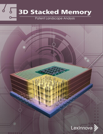
3D Stacked Memory: Patent Landscape Analysis
Table of ContentsExecutive Summary . .1Introduction . .2Filing Trend . .7Taxonomy . . . 8Top Assignees . . . 11Geographical Heat Map . .13LexScoreTM . . . 14Patent Strength . . .16Licensing Heat Map . . .17Appendix: Definitions . .193D Stacked Memory: Patent Landscape Analysis
EXECUTIVE SUMMARYMemory bandwidth, latency and capacity have become a major performance bottleneck as more andmore performance and storage are getting integrated in computing devices, demanding more datatransfer between processor and system memory (Volatile and Non-Volatile). This memory bandwidthand latency problem can be addressed by employing a 3D-stacked memory architecture which providesa wide, high frequency memory-bus interface. 3D stacking enables stacking of volatile memory likeDRAM directly on top of a microprocessor, thereby significantly reducing transmission delay betweenthe two. The 3D- stacked memory also improves memory capacity and cost of non-volatile storagememory like flash or solid state drives. By stacking, memory dies vertically in a three-dimensionalstructure, new potential for 3D memory capacities are created, eliminating performance and reliabilityissues from capacity limitations.In this report, we study the Intellectual Property (Patents) landscape of this fast growing technology. Wefind that the majority of patenting activity has occurred in technologies related to wafer manufacturingprocesses step BEOL and FEOL with impact on design parameters such as, ‘Structural Features’, ‘ModelParameters’, ‘Operating Speed’. We also find that majority of the patents/patent applications aredistributed among top three companies. The share of these top three assignees is around 52% of thetotal patents/patent applications (considered for analysis) in this technology domain. SanDisk is at thetop and holds around 34% of the total patents followed by Micron and Samsung. The US geography hasseen the maximum patent filings and, is followed by the other big markets such as China, Japan, SouthKorea and Taiwan.Using our proprietary patent analytics tool, LexScoreTM, we identify SanDisk as the leader in thistechnology domain with good patent portfolio quality as well as quantity. Micron also holds a largenumber of patents in this domain. The combination of patent holding pattern and a high patent filingactivity suggest a significant potential for patent licensing activity in this technology domain. Using ourproprietary Licensing Heat-map framework, we predict 3D memory stacking technology sub domains forlicensing activity.The top assignee, SanDisk shares a fabrication plant with Toshiba which also appears among the topseven assignees in this technology. Samsung is working on its own 3D stacked memory and has releasedseveral iterations till now. Several companies are entering into partnerships to use each other’sresources. On the other hand, Guobiao Zhang is the individual inventor of 57 patents/patentapplications in 3D stacked memory technology. Micron Technology with its existing partnership withIntel plans to release 10TB flash memory in a 2mm chip by the end of this year.In the following sections, we present our analysis of the Patent Landscape of this technology domain.Page 13D Stacked Memory: Patent Landscape Analysis
INTRODUCTIONWith the increased demand for enhanced functionality and miniaturization inportable hand-held devices such as cell phones, digital cameras and laptops—equipment manufacturers have focused on reducing the component footprint inassembling these devices. Processors and storage memories (volatile and nonvolatile) are two most important ingredients in manufacturing computingdevices that determine form factor and functionality. The memory needs formodern portable devices requires high capacity, low latency and compact formfactor. This requires not only innovative nanoscale memory cell designs but alsoinnovative packaging technologies to provide high capacity with compact size.Silicon chip manufacturers have turned to 3D memory stacking solutions toprovide high capacity and smaller size. Stacking of multiple memory chips, notonly provides a reduction in overall package footprint, but also a significantimprovement in electrical performance due to shorter interconnects. Thisfacilitates quicker signal transmission (low data latency) requiring less energy todrive the signals. This enables a new generation of tiny but powerful deviceswith high storage capacity and performance.The memory and processor always co-exist in a computing device. Theprocessor has controller that communicates with the memory. The memory andprocessors are usually designed in different manufacturing process technologynodes due to cost and performance advantages. If transistors get any smaller,their reliability could become questionable and the cost of manufacturing in sub28nm node is much higher. Such issues have led to the adoption of threedimensional (3D) integrated circuit manufacturing technology, where two ormore dice are stacked atop each other and linked with suitable interconnects.The primary benefit is that the electrical interconnects between blocks areshorter apart from compact size. This lowers power dissipation and operationallatency since fewer buffers, flip-flops and shorter transmission lines are needed.Reducing the amount of metal that runs across the chip also reduces powerdissipation. Lower inter-block latency reduces cycle time, increasesresponsiveness and chip performance. Stacking layers also increases chipdensity, as more transistors are able to be placed per unit of volume and withinone clock cycle of each other.There are three main ways of stacking chips; the first technique involvesstacking two chips together, and then connecting them through flip chipbonding at the bottom of the stack. This technique can be used to place DRAMon the top of a CPU. The second technique is called through-silicon via (TSV).With TSV, vertical copper channels are built into each die, so that when they’replaced on top of each other, the TSVs connect the chips together (as shown inthe figure). This is the technique that was initially developed by IBM. CMOSimage sensors were first to adopt TSV in high volume manufacturing. Thesehave seen resurgence due to need for compact size in smartphones, tablets andIBM, ÉcolePolytechniqueFédérale deLausanne (EPFL)and the SwissFederal Institute ofTechnology Zurich(ETH) signed afour-yearcollaborativeproject calledCMOSAIC tounderstand howthe latest chipcooling techniquescan support a 3Dchip architecture.Nvidia is usingwhat is calledVertical stacking3D, or on-packagestacked DRAM forits Pascal 2016GPUs.Page 23D Stacked Memory: Patent Landscape Analysis
laptops. TSV’s allow for stacking of volatile memory DRAM with processor(memory controller) to build very compact devices for portable applications.This technique also allows 3D stacking of memory chip to create dense nonvolatile memory like flash or solid state drives with high capacity.Figure 1: 3D Memory Stack using TSV technique1The third technique is advanced packaging method which uses a silicontransposer. A transposer is effectively a piece of silicon that acts like a minimotherboard, connecting two or more chips together. The advantage of thistechnique is that you can have shorter wiring (higher bandwidth, lower powerconsumption), but the constituent chips can be of different manufacturingtechnology or type. Transposers are expected to be used in upcoming multiGPU Nvidia and AMD graphics cards.The second technique called through-silicon-via (TSV) is most widely used forstacking memory chips. This is essentially a wafer level packaging method wherea via goes from the front side of the wafer (typically connecting to one of thelower metal layers) through and out to the back. TSVs vary in diameter from1um to 10um, with a depth of 5 to 10 times the width. A hole is formed into thewafer, lined with an insulator, and then filled with copper or tungsten. Thewafer is thinned to expose the backside of the TSVs. The wafer is thinned usingCMP (chemical mechanical polishing) until the TSVs are almost exposed. Moresilicon is then etched away to reveal the TSVs themselves. FEOL (front-end ofline) in fab manufacturing is where transistors are created. BEOL (back-end ofline) is where interconnects between transistors are created. TSV’s can bemanufactured in three different ways. TSVfirst (build them before thetransistors/FEOL) and TSVlast (build them after BEOL). In TSVmiddle process,the TSVs are formed between transistors and interconnects. TSV first is nolonger viable due to high via resistances. TSV last approach has been popular inCMOS image sensors due to need for high aspect ratio. This method is1ThruChipCommunications'ThruChip Interface(TCI) utilizesinductive curlsthat impart layerto-layer asopposed to thephysical metalwires utilized bythrough-silicon bymeans of (TSV)tech to connectiona 3D chip's siliconlayers.Toshiba andSanDisk announceBiCS as the first48-layer 3D flashchip.Chip-to-Chip Input/Output (I/O) Thrust, Advanced Computing Systems GroupPage 33D Stacked Memory: Patent Landscape Analysis
challenging for high-density 3D IC applications. TSVmiddle is more commerciallyviable and popular method for 3D stacking of integrated circuits. In this methodafter interconnects creation the micro bumps are created. The wafer is glued toa glass carrier. The back is then grinded down and a passivation layer is applied.This is then etched to expose the TSVs and then micropads are created. Thefigure below shows the TSVmiddle approach of manufacturing flow.TSVs are utilized,for instance, inMicron's HybridMemory Cube(HMC) andSamsung'svertically stackedNAND (V-NAND)chips, and areunderconcentrated studyby various chipcreators andfabricators.Figure 2: 3D TSV process flow2The growing importance of 3D stacking in industry has led to an extensiveresearch in this area. Applied Materials (manufacturing equipment maker forIntel, TSMC, Samsung, Global Foundries, and other foundries) and A*STAR'sInstitute of Microelectronics (IME) have declared the opening of a forefront 3Dchip bundling lab in Singapore. Assembled with a consolidated speculation ofover 100 million, the Center of Excellence in Advanced Packaging highlights a14,000 square foot cleanroom containing a finish 300-millimeter creation lineand 3D bundling instruments that are novel to A*STAR.In 2004, Intel3 presented a 3D version of the Pentium 4 CPU. The chip wasmanufactured with two dice using face-to-face stacking, which allowed a densevia structure. Backside TSVs were used for I/O and power supply. For the 3Dfloor-plan, designers manually arranged functional blocks in each die aiming forpower reduction and performance improvement. Splitting of large and highpower blocks and careful rearrangement limited thermal hotspots. The 3D23The worldwide 3DIC market isexpected todevelop from 2.21billion in 2009 to 6.55 billion in2015 at a CAGR of16.9% from 2011to 2015.TSV MEOL Process Flow for Mobile 3D IC Stacking, 3dincites.com, August 7, 2014Generations of the computer processors, Piotr GwizdałaPage 43D Stacked Memory: Patent Landscape Analysis
design provided 15% performance improvement (due to eliminated pipelinestages) and 15% power saving (due to eliminated repeaters and reduced wiring)as compared to the 2D Pentium 4.The Teraflops Research Chip4, introduced in 2007 by Intel was an experimental80-core design with stacked memory. Due to the high demand for memorybandwidth, a traditional I/O approach would consume 10 to 25 W. To improveupon that, Intel designers implemented a TSV-based memory bus. Each core isconnected to one memory tile in the SRAM die with a link that provides 12 GB/sbandwidth, resulting in a total bandwidth of 1 TB/s while consuming only 2.2 W.As market players compete to realize the huge economic potential offered bythe 3D stacking, we have seen M&A, partnerships and product announcementsin 3D memory stacking technology domain. Intel and its partner Micronannounced 3D NAND solution that enables chips with 384Gbit (48GB) ofcapacity which is three times to that of existing 3D NAND parts. Along withhigher densities, Intel/Micron promise lower costs, improved read/writeperformance, and new sleep modes that cut power to inactive parts of a chip.The offerings take aim at Samsung, which has been shipping 3D NAND memoryparts for several months, as well as Toshiba and its partner SanDisk. AMD hasreported that it would be mutually working with memory device manufacturer,SK Hynix, in the development of cutting edge High-bandwidth 3D stackedmemory items and arrangements.SanDisk's recent profit5 warning shows potential headwinds in the NAND Flashmemory space, which represents to 28% of Micron's income. Samsung's new 14.7B chip production line has a high probability of upsetting the fragilesupply-demand balance in the DRAM business, which represents 68% ofMicron's income.The worldwide 3D IC market is expected to grow from 2.21 billion in 2011 to 6.55 billion in 2015 at a CAGR of 16.9% from 2011 to 2015. The organizations inthis business need to productively adjust their expenditure between capacityextension and research & development. This is viewed as critical for subsequentsustainability and growth for 3D ICs business. This balance is driven bypenetration of 3D-stached memory into computing devices. Following figureshows this.45Intel and itspartner Micron,announced 3DNAND solution thatenables chips with384Gbit (48GB) ofcapacity which isthree times to thatof existing 3DNAND parts.AMD has reportedthat it would bemutually workingwith memorydevicemanufacturer, SKHynix, in thedevelopment ofcutting edge Highbandwidth 3Dstacked memoryitems andarrangements.Intel Details 80-Core Teraflops Research Chip, xbitlabs.com, Anton Shilov, February 12, 2007Micron: This Time Is Not Different, Seeking Alpha, January 16, 2015Page 53D Stacked Memory: Patent Landscape Analysis
Figure 3: Global 3D TSV device market value6In such a high growth and fast evolving market, safeguarding a company’sinterest using Intellectual property is an important strategy for market players.Assessing the IP landscape is therefore an important exercise for current marketplayers as well as companies who are looking to enter this market. In thefollowing paragraphs we analyze the patent landscape of 3D Memory Stacking.6Spotlight on 3D-IC, 450mm Wafer Transition, and MEMS — SEMICON Taiwan 2012 Preview, semi.org, August 7, 2012Page 63D Stacked Memory: Patent Landscape Analysis
Filing TrendIn 2004, TezzaronSemiconductorbuilt working 3Ddevices from sixdifferent designs.The chips werebuilt in two layerswith "via-first"tungsten TSVs forverticalinterconnection.Figure below shows the number of patent/patents applications related to 3Dstacked memory between 1995 and 2014. The IP activity has seen steadyincrease from 1995 to 2005 with a sharp rise in 2006. The patent activity nearlydoubled from 99 in 2005 to 198 in 2006. In 2006, SanDisk increased its IP filingactively in this domain which resulted in the spike. The filing activity tapered offbetween 2006 and 2010 due to economic downturn but picked off postrecession, increasing from 175 in 2010 to 283 in 2012. The 2013 & 2014 trendsshow lower number because the full published data is not available till now andthe numbers are incomplete. This does not imply that patent filings in 2013 &2014 have actually gone 950Figure 4: Filing TrendPage 73D Stacked Memory: Patent Landscape Analysis
Taxonomy3D memory stacking technology exploits the third or Z height dimension toprovide a volumetric packaging solution for higher integration and performance.3D stacking has become critical for enhancing the multi-media featuresconsumers demand in smaller, lighter products. This increasing functionalityrequires higher memory capacity in more compact size. New product designs(cell phones, digital cameras, PDAs, audio players and mobile gaming) demanddiverse feature set in innovative form factor and styling. 3D stacking enablesthese designs with highest level of device integration, area efficiency at a lowcost. The taxonomy is presented in the form of a 2D matrix with manufacturingprocesses on one axis and design parameters on the other. The taxonomyfocuses on the impact of various manufacturing processes on the designparameters. The categorization of patents/patent applications, related to 3Dmemory stacking was done on the basis of manufacturing processes and theaffected design parameters. The set considered for the analysis comprised ofaround 2,300 patents/patent applications.The manufacturing process is divided into FEOL (Front-end-of-line), BEOL (Backend-of-line), Assembly and Testing. 3D stacked memory technology impactsBEOL & FEOL manufacturing the most as most building happens there. Mostpatents/patent applications fall in BEOL & FEOL manufacturing process. Due tothis, FEOL is further divided into processes involved in the manufacturing ofdevices, such as Wafer Development, Oxide Growth, Lithography, Etching,Device Formation, Stacking and Others. Also, BEOL is further divided intoprocesses involved in the manufacturing of devices, such as Metal LayerFormation, Interconnects Formation, Contact Formation, and Others.Stanfordengineers havebuild 3D “highrise” chips thatcould leapfrog theperformance ofthe single-storylogic and memorychips on today’scircuit cards,which are subjectto frequent trafficjams betweenlogic and memory.The design parameters are classified as Structural features, Design Flow, ModelParameters, Power Consumption, Feature Size, Operating Voltage, OperatingSpeed and leakage current.Please refer to Appendix for detailed definitions of the various categories.Page 83D Stacked Memory: Patent Landscape Analysis
Figure 5: TaxonomyIn the manufacturing processes category, FEOL and BEOL are of interest. Thereare 1468 patents/patent applications in FEOL, and 1549 in BEOL. In FEOLcategory, the following sub-domains are of interest: Stacking, Etching andDevice Formation. There are 899 patents/patent applications in ‘Stacking’, 395in ‘Etching’, and 322 in ‘Device Formation’. There are some patents/patentapplications that cover multiple manufacturing processes and multiple designparameters.In the design parameters category, the following sub-domains are of interest:Structural Features, Model Parameters, Operating Voltage, and OperatingSpeed. There are 1743 patents/patent applications in ‘Structural features’, 523in ‘Model Parameters’, 357 in ‘Operating Voltage, and 311 in ‘Operating Speed’.Stacking is an important step in the formation of 3D stacked memory. In thisprocess, the individual devices are stacked on the top of other devices and areinterconnected by metallic interconnects.Etching is a critically important process in the manufacturing of a 3D memorystack. Every wafer undergoes many etching steps before the manufacturing iscomplete. Etching is used to chemically remove layers from the surface of awafer during fabrication. The part of the wafer is protected from the etchant bya mask which resists etching.Device Formation refers to the formation of gate, source and drain on thesubstrate layer. Gate film is formed by oxidation and then, plasma nitridationprocess is applied to the surface of the gate film. Gate electrode (polysilicon) isformed on it by CVD (Chemical Vapor Deposition) method. The impurities(specific elements) are diffused into the substrate by ion-implantation to formsource and drain.Samsung has hugearrangements forfuture emphasesof the V-NANDtech,incorporating 3Dchips with up to24 layers, allassociated byutilizing "uniquecarvinginnovation" tobore downthrough the layersand interface themelectronically.Page 93D Stacked Memory: Patent Landscape Analysis
Structural features refer to the structural components of devices. Since 3D stackmemory technology is functionally a passive interconnect structure so most ofthe patents/patent applications fall under structural feature.Model Parameters refer to electrical characteristics of 3D stack memorytechnology. These parameters have a great impact on the performance of aninterconnect, is an important factor in 3D stack memory technology.Operating voltage and Operating speed are important design parameters in 3Dstack memory technology . Operating Voltage is the minimum voltage requiredfor the proper operation of a device and Operating speed refers to the timetaken by a device to generate the output after an input is applied to it.SanDisk's recentprofit warningshows potentialheadwinds in theNAND Flashmemory space,which representsto 28% of Micron'sincomes.Page 103D Stacked Memory: Patent Landscape Analysis
Top AssigneesFigure below depicts the top assignees having patents/patent applicationsrelated to 3D Stacked Memory Technology.SanDisk, Micron and Samsung are the top three assignees with 793, 219 and 194patents/patent applications respectively. The numbers of patents/patentapplications owned by top three assignees comprise around 52% of the totalpatents/patent applications (around 2,300) filed in the domain which areconsidered in the analysis. Guobiao Zhang is an individual inventor who has 57patents/patent applications.The top assignee, SanDisk shares a fabrication plant with Toshiba which alsoappears among the top seven assignees in this technology. Samsung is workingon its own 3D stacked memory and has released several iterations till now.Several companies are entering into partnerships to use each other’s resources.On the other hand, Guobiao Zhang is the individual inventor of 57patents/patent applications in 3D stacked memory technology. MicronTechnology, in partnership with Intel, is planning to release memory of 10TBflash memory in a 2mm chip by the end of this year.The R & D expenses of SanDisk in the last 3 years are US 602.8, US 742.3 andUS 852.3 million and that of Micron, US 918, US 931 and US 1,371 millionand that of Samsung, US 212.29, US 304.66 and US 327.73 millionrespectively. This shows that R & D expenses of all the top assignees haveincreased since last 3 years and are expected to increase more. Moreover, therevenues of all the companies are also increasing. For Sandisk, revenuesincreased from US 5052.5 to US 6,627.7 million between 2012 and 2014 andfor Micron, revenues increased from US 8,234 to US 16,358 million and forSamsung, revenues decreased from US 7177.57 to US 6479.95 millionrespectively.The Low PowerMemoriesSubcommittee (JC42.6) haspublished astandard for WideI/O Mobile DRAMwith TSVinterconnectsstacked on Systemon a Chip (SoC)ApplicationProcessors.Figure 6: Top AssigneesPage 113D Stacked Memory: Patent Landscape Analysis
The maximum number of patents/patent applications filings has been done in the year 2006 and 2007by SanDisk. The companies listed in following table can be termed as top leaders in terms of their patentportfolio.Table 1: Top Assignees year-wise trendPage 123D Stacked Memory: Patent Landscape Analysis
Geographical Heat MapThe United States has seen maximum number of patent filings in domain of 3Dstacked memory technology. China, Japan, Korea and Taiwan have also seengood number of patent filings.SanDisk is the top assignee with 793 patent/patents applications with 412 in theUnited States. Samsung has 18 patent/patents applications in China where as anindividual inventor Guobiao Zhang has 16. The 3D memory patents/patentapplications are concentrated in traditional memory manufacturing countrieslike US, China, Japan, Korea and Taiwan.Toshiba is tryingto leapfrogSamsung’smaximum densitywith 48-layermemory, asopposed to theKoreanmanufacturer’scurrent 32-layerdesigns.Figure 7: Geographical Heat MapPage 133D Stacked Memory: Patent Landscape Analysis
LexScoreTMWe use LexInnova’s proprietary LexSoreTM framework to identify strength ofintellectual property portfolio in 3D stacked memory domain. Figure belowdepicts the competitive positioning of top 15 assignees, in 3D Stacked Memorydomain. The assignees are compared on the basis of filing score and qualityscore. We use our proprietary algorithm (based on bibliographical informationand claim characteristics of an invention) to calculate and rank the quality ofinventions.The green region comprises of the assignees with the best patent portfolios,which are exemplary in terms of quality and number of patents. SanDisk is theonly assignee lying in the green domain. It can be safely assumed that has thebest intellectual property portfolio in area of 3D memory.Matrix SemiconductorHitachiSandiskPortfolio Quality ScoreGuobiao ZhangHPToshibaSharpMacronixIntelMicron TechnologySamsungIII HoldingsUnity semiconductorIBMAMDPortfolio Filing ScoreFigure 8: LexScoreTMThe blue region contains assignees that possess good quality patents but lack onthe patent filing quantity front. Matrix Semiconductor, HP, Hitachi and GuobiaoZhang lie in this region. They have good quality inventions in this domain butthey lack numbers due to their reduced patent filing in the previous five years.Matrix Semiconductor has maximum number of quality patents owing to largenumber of patents citations assigned their patents. Patents filed by Hitachi havethe best technological coverage.Page 143D Stacked Memory: Patent Landscape Analysis
Most of the assignees form a cluster in the red region with patent portfoliolacking on both patent quality and quality of filing. IBM, Unity Semiconductor,and AMD have filed most of their patents within past three years (2012-14);hence the patents quality is hampered. Their patent portfolio may rise in futureafter successful prosecution of their patents that are in pipeline and morecitations may get added. Patents assigned to III Holdings have the lowestgeographical score as they have filed their patents/patent applications only inthe USA.Page 153D Stacked Memory: Patent Landscape Analysis
Patent StrengthThe patents in our report are ranked programmatically by our proprietary toolthat relies on the algorithm developed by Mark A. Lemley, Kimberly A. Moore,John R. Allison, R. Derek Trunkey in their research paper, "Valuable Patents".Historical research has proven that 97% of the litigation-worthy patents in aportfolio are found in Top 30 percentile of the patents ranked by using thisalgorithm.SanDisk has 214 patents in Top 30 percentile, which is the maximum for anycompany related to this sector. Micron has 33 which is very low as compared toits competitor SanDisk. NPE’s like Intellectual Ventures, Qimonda AG and RoundRock Research LLC have 6, 5 and 5 patents in Top 30 percentile.21433241766555444Figure 9: Companies with maximum number of litigation-worthy patentsPage 163D Stacked Memory: Patent Landscape Analysis
Licensing Heat MapWe use our LexInnova’s Licensing-Heat Map (Figure below) framework toidentify technology sub-domains in the field of 3D stacked memory technologywhere licensing activity is expected to be higher. The size of the sections(representing different technology domains) in the Heat Map indicates thenumber of patents/patent applications filed in this domain. It also implies therelative importance of the technology sub-domain. The color scheme hererepresents the chances of future licensing activity in this domain. We study thepatent holding pattern to color code the technology sub-domain for futurelicensing activity.Red color (and shades thereof) signifies a high likelihood of licensing activity in acertain technology sub-domain whereas the green color (and shades thereof)represents a low likelihood. We follow 80-20 rule to decide the colors, yellow isassigned to the domains that lie on the average case (i.e. 20% assignees having80% of the patents/patent applications). The color drifts towards shades of redif 20% assignees possess less than 80% of the patents/patent applications, whileit drifts towards shades of green in the reverse case.JEDEC disclosedthe upcomingDRAM technologyincludes the "3DSiC" die stackingplan at "ServerMemory Forum",November 1–2,2011, Santa Clara,CA.Figure 10: Licensing Heat Map*Contact Formation Operating Speed**Contact Formation Model ParametersPage 173D Stacked Memory: Patent Landscape Analysis
Sub domains like Stacking, BEOL and Etching combined with the structuralfeatures have the highest number of patent/patent applications in the 3Dstacked memory technology while domains like Model Parameters, OperatingSpeed and FEOL with structural features has relatively lesser number ofpatent/patent applications. As mentioned above, sub domains which are darkred in the heat map have higher chances of licensing activity as compared todomains which fall in the lighter shades. Model parameters related to contactformation (FEOL) and Operating Speed in contact formation (FEOL) andstructural features related to Assembly/Packaging are red in color which reflectsa very distributed portfolio with no monopoly of any assignee in these domains.While domains like Stacking, BEOL and Etching combined with the structuralfeatures fall in the lighter shades reflecting that the patent portfolio in thesedomains is predominantly held by some top players.Intel, Sun vetbirths fast,inexpensive 3Dchip-stackingbreakthrough.Major Players in the contact formation related to operating speed technologydomains are Micron Technology, Samsung, Intel, III Holdings, Guobiao Zhang.Major Players in the FEOL related to structural features technology domains areSanDisk, Samsung, Macronix. Major Pla
laptops. TSVs allow for stacking of volatile memory DRAM with processor (memory controller) to build very compact devices for portable applications. This technique also allows 3D stacking of memory chip to create dense non-volatile memory like flash or solid state drives with high capacity. Figure 1: 3D Memory Stack using TSV technique1

