Transcription
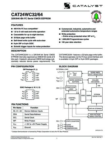
HCAT24WC32/64EEGEN FRALO32K/64K-Bit I2C Serial CMOS EEPROMLEA D F R E ETMFEATURES 400 KHz I2C bus compatible* Commercial, industrial, automotive andextended automotive temperature ranges 1.8 to 6 volt read and write operation Write protection Cascadable for up to eight devices– Entire array protected when WP at VIH 32-Byte page write buffer 1,000,000 Program/erase cycles Self-timed write cycle with auto-clear 100 year data retention 8-pin DIP or 8-pin SOIC Schmitt trigger inputs for noise protectionDESCRIPTIONThe CAT24WC32/64 is a 32K/64K-bit Serial CMOSE2PROM internally organized as 4096/8192 words of 8bits each. Catalyst’s advanced CMOS technology substantially reduces device power requirements. TheCAT24WC32/64 features a 32-byte page write buffer.The device operates via the I2C bus serial interface andis available in 8-pin DIP or 8-pin SOIC packages.PIN CONFIGURATIONBLOCK DIAGRAMDIP Package (P, L)A0A11287VCCWPA2VSS3465SCLSDAEXTERNAL LOADSENSE AMPSSHIFT REGISTERSDOUTACKVCCWORD ADDRESSBUFFERSVSSCOLUMNDECODERS256SOIC Package (J, W, K, PROMXDEC 128/256 128/256 X 256CONTROLLOGICWPPIN FUNCTIONSPin NameFunctionA0, A1, A2Device Address InputsSDASerial Data/AddressSCLSerial ClockWPWrite ProtectVCC 1.8V to 6V Power SupplyVSSGroundDATA IN STORAGEHIGH VOLTAGE/TIMING CONTROLSCLA0A1A2STATE COUNTERSSLAVEADDRESSCOMPARATORS24WC32/64 F02* Catalyst Semiconductor is licensed by Philips Corporation to carry the I2C Bus Protocol. 2004 by Catalyst Semiconductor, Inc.Characteristics subject to change without notice1Doc. No. 1039, Rev. F
CAT24WC32/64ABSOLUTE MAXIMUM RATINGS**COMMENTTemperature Under Bias . –55 C to 125 CStresses above those listed under “Absolute MaximumRatings” may cause permanent damage to the device.These are stress ratings only, and functional operation ofthe device at these or any other conditions outside of thoselisted in the operational sections of this specification is notimplied. Exposure to any absolute maximum rating forextended periods may affect device performance andreliability.Storage Temperature . –65 C to 150 CVoltage on Any Pin withRespect to Ground(1) . –2.0V to VCC 2.0VVCC with Respect to Ground . –2.0V to 7.0VPackage Power DissipationCapability (Ta 25 C) . 1.0WLead Soldering Temperature (10 secs) . 300 COutput Short Circuit Current(2) . 100mARELIABILITY ence Test Method1,000,000Cycles/ByteMIL-STD-883, Test Method 1033Data Retention100YearsMIL-STD-883, Test Method 1008ESD Susceptibility2000VoltsMIL-STD-883, Test Method Max.JEDEC Standard 17D.C. OPERATING CHARACTERISTICSVCC 1.8V to 6.0V, unless otherwise st ConditionsICCPower Supply Current3mAfSCL 100 KHzISB(5)Standby Current (VCC 5V)1µAVIN GND or VCCILIInput Leakage Current10µAVIN GND to VCCILOOutput Leakage Current10µAVOUT GND to VCCVILInput Low Voltage–1VCC x 0.3VVIHInput High VoltageVCC x 0.7VCC 0.5VVOL1Output Low Voltage (VCC 3.0V)0.4VIOL 3.0 mAVOL2Output Low Voltage (VCC 1.8V)0.5VIOL 1.5 mACAPACITANCE TA 25 C, f 1.0 MHz, VCC 5VSymbolTestMax.UnitsConditionsCI/O(3)Input/Output Capacitance (SDA)8pFVI/O 0VCIN(3)Input Capacitance (A0, A1, A2, SCL, WP)6pFVIN 0VNote:(1) The minimum DC input voltage is –0.5V. During transitions, inputs may undershoot to –2.0V for periods of less than 20 ns. Maximum DCvoltage on output pins is VCC 0.5V, which may overshoot to VCC 2.0V for periods of less than 20ns.(2) Output shorted for no more than one second. No more than one output shorted at a time.(3) This parameter is tested initially and after a design or process change that affects the parameter.(4) Latch-up protection is provided for stresses up to 100 mA on address and data pins from –1V to VCC 1V.(5) Maximum standby current (ISB ) 10µA for the Automotive and Extended Automotive temperature range.Doc. No. 1039, Rev. F2
CAT24WC32/64A.C. CHARACTERISTICSVCC 1.8V to 6V, unless otherwise specifiedOutput Load is 1 TTL Gate and 100pFRead & Write Cycle Limits1.8V - 6.0 V2.5V - SCLClock Frequency100400kHzTI(1)Noise Suppression TimeConstant at SCL, SDA Inputs200200nstAASCL Low to SDA Data Outand ACK Out3.51µstBUF(1)Time the Bus Must be Free Beforea New Transmission Can StarttHD:STAStart Condition Hold TimetLOW4.71.2µs40.6µsClock Low Period4.71.2µstHIGHClock High Period40.6µstSU:STAStart Condition Setup Time(for a Repeated Start Condition)4.70.6µstHD:DATData In Hold Time00nstSU:DATData In Setup Time5050nstR(1)SDA and SCL Rise Time10.3µstF(1)SDA and SCL Fall Time300300nstSU:STOStop Condition Setup TimetDHData Out Hold Time40.6µs100100nsPower-Up Timing (1)(2)SymbolParameterMax.UnitstPURPower-Up to Read Operation1mstPUWPower-Up to Write Operation1msNote:(1) This parameter is tested initially and after a design or process change that affects the parameter.(2) tPUR and tPUW are the delays required from the time VCC is stable until the specified operation can be initiated.Write Cycle LimitsSymbolParametertWRWrite Cycle TimeMin.The write cycle time is the time from a valid stopcondition of a write sequence to the end of the internalprogram/erase cycle. During the write cycle, the busTyp.MaxUnits10msinterface circuits are disabled, SDA is allowed to remainhigh, and the device does not respond to its slaveaddress.3Doc. No. 1039, Rev. F
CAT24WC32/64FUNCTIONAL DESCRIPTIONSDA: Serial Data/AddressThe bidirectional serial data/address pin is used totransfer all data into and out of the device. The SDA pinis an open drain output and can be wire-ORed with otheropen drain or open collector outputs.The CAT24WC32/64 supports the I2C Bus data transmission protocol. This Inter-Integrated Circuit Bus protocol defines any device that sends data to the bus to bea transmitter and any device receiving data to be areceiver. The transfer is controlled by the Master devicewhich generates the serial clock and all START andSTOP conditions for bus access. The CAT24WC32/64operates as a Slave device. Both the Master device andSlave device can operate as either transmitter or receiver, but the Master device controls which mode isactivated.A0, A1, A2: Device Address InputsThese pins are hardwired or left unconnected (for hardware compatibility with CAT24WC16). When hardwired,up to eight CAT24WC32/64s may be addressed on asingle bus system (refer to Device Addressing ). Whenthe pins are left unconnected, the default values arezeros.WP: Write ProtectThis input, when tied to GND, allows write operations tothe entire memory. For CAT24WC32/64 when this pinis tied to Vcc, the entire memory is write protected.When left floating, memory is unprotected.PIN DESCRIPTIONSSCL: Serial ClockThe serial clock input clocks all data transferred into orout of the device.Figure 1. Bus :DATtSU:STOSDA INtAAtBUFtDHSDA OUT5020 FHD F03Figure 2. Write Cycle TimingSCLSDA8TH BITBYTE nACKtWRSTOPCONDITIONSTARTCONDITIONADDRESS5020 FHD F04Figure 3. Start/Stop TimingSDASCLSTART BITDoc. No. 1039, Rev. FSTOP BIT45020 FHD F05
CAT24WC32/64I2C BUS PROTOCOLcompare to the hardwired input pins, A2, A1 and A0. Thelast bit of the slave address specifies whether a Read orWrite operation is to be performed. When this bit is setto 1, a Read operation is selected, and when set to 0, aWrite operation is selected.The features of the I2C bus protocol are defined asfollows:(1) Data transfer may be initiated only when the bus isnot busy.After the Master sends a START condition and the slaveaddress byte, the CAT24WC32/64 monitors the bus andresponds with an acknowledge (on the SDA line) whenits address matches the transmitted slave address. TheCAT24WC32/64 then performs a Read or Write operation depending on the state of the R/W bit.(2) During a data transfer, the data line must remainstable whenever the clock line is high. Any changesin the data line while the clock line is high will beinterpreted as a START or STOP condition.START ConditionAcknowledgeThe START Condition precedes all commands to thedevice, and is defined as a HIGH to LOW transition ofSDA when SCL is HIGH. The CAT24WC32/64 monitorsthe SDA and SCL lines and will not respond until thiscondition is met.After a successful data transfer, each receiving device isrequired to generate an acknowledge. The Acknowledging device pulls down the SDA line during the ninth clockcycle, signaling that it received the 8 bits of data.The CAT24WC32/64 responds with an acknowledgeafter receiving a START condition and its slave address.If the device has been selected along with a writeoperation, it responds with an acknowledge after receiving each 8-bit byte.STOP ConditionA LOW to HIGH transition of SDA when SCL is HIGHdetermines the STOP condition. All operations must endwith a STOP condition.When the CAT24WC32/64 begins a READ mode ittransmits 8 bits of data, releases the SDA line, andmonitors the line for an acknowledge. Once it receivesthis acknowledge, the CAT24WC32/64 will continue totransmit data. If no acknowledge is sent by the Master,the device terminates data transmission and waits for aSTOP condition. The master must then issue a stopcondition to return the CAT24WC32/64 to the standbypower mode and place the device in a known state.DEVICE ADDRESSINGThe bus Master begins a transmission by sending aSTART condition. The Master sends the address of theparticular slave device it is requesting. The four mostsignificant bits of the 8-bit slave address are fixed as1010 (Fig. 5). The next three bits (A2, A1, A0) are thedevice address bits; up to eight 32K/64K devices mayto be connected to the same bus. These bits mustFigure 4. Acknowledge TimingSCL FROMMASTER189DATA OUTPUTFROM TRANSMITTERDATA OUTPUTFROM RECEIVERACKNOWLEDGESTART5020 FHD F06Figure 5. Slave Address Bits1010A2A1A0R/W5027 FHD F075Doc. No. 1039, Rev. F
CAT24WC32/64If the Master transmits more than 32 bytes before sendingthe STOP condition, the address counter ‘wraps around’,and previously transmitted data will be overwritten.WRITE OPERATIONSByte WriteIn the Byte Write mode, the Master device sends theSTART condition and the slave address information(with the R/W bit set to zero) to the Slave device. Afterthe Slave generates an acknowledge, the Master sendstwo 8-bit address words that are to be written into theaddress pointers of the CAT24WC32/64. After receivinganother acknowledge from the Slave, the Master devicetransmits the data to be written into the addressedmemory location. The CAT24WC32/64 acknowledgesonce more and the Master generates the STOP condition. At this time, the device begins an internal programming cycle to nonvolatile memory. While the cycle is inprogress, the device will not respond to any request fromthe Master device.When all 32 bytes are received, and the STOP conditionhas been sent by the Master, the internal programmingcycle begins. At this point, all received data is written tothe CAT24WC32/64 in a single write cycle.Acknowledge PollingDisabling of the inputs can be used to take advantage ofthe typical write cycle time. Once the stop condition isissued to indicate the end of the host's write operation,CAT24WC32/64 initiates the internal write cycle. ACKpolling can be initiated immediately. This involves issuing the start condition followed by the slave address fora write operation. If CAT24WC32/64 is still busy with thewrite operation, no ACK will be returned. IfCAT24WC32/64 has completed the write operation, anACK will be returned and the host can then proceed withthe next read or write operation.Page WriteThe CAT24WC32/64 writes up to 32 bytes of data, in asingle write cycle, using the Page Write operation. Thepage write operation is initiated in the same manner asthe byte write operation, however instead of terminatingafter the initial byte is transmitted, the Master is allowedto send up to 31 additional bytes. After each byte hasbeen transmitted, CAT24WC32/64 will respond with anacknowledge, and internally increment the five low orderaddress bits by one. The high order bits remain unchanged.WRITE PROTECTIONThe Write Protection feature allows the user to protectagainst inadvertent programming of the memory array.If the WP pin is tied to VCC, the entire memory array isprotected and becomes read only. The CAT24WC32/64will accept both slave and byte addresses, but theFigure 6. Byte Write TimingBUS ACTIVITY:MASTERSDA LINESTARTSLAVEADDRESSBYTE ADDRESSA15–A8A7–A0SSTOPDATAPX XX *ACKACKACKACK24WC32/64 F08Figure 7. Page Write TimingBUS ACTIVITY:MASTERSDA LINESTARTSLAVEADDRESSBYTE ADDRESSA15–A8A7–A0SDATADATA n 31PX XX *ACKACKACK* Don't care bit for 24WC32X Don't care bitDoc. No. 1039, Rev. FDATA nSTOPACKACKACKACK24WC32/64 F096
CAT24WC32/64‘dummy’ write operation by sending the START condition, slave address and byte addresses of the location itwishes to read. After CAT24WC32/64 acknowledges,the Master device sends the START condition and theslave address again, this time with the R/W bit set to one.The CAT24WC32/64 then responds with its acknowledge and sends the 8-bit byte requested. The masterdevice does not send an acknowledge but will generatea STOP condition.memory location accessed is protected from programming by the device’s failure to send an acknowledgeafter the first byte of data is received.READ OPERATIONSThe READ operation for the CAT24WC32/64 is initiatedin the same manner as the write operation with oneexception, that R/W bit is set to one. Three differentREAD operations are possible: Immediate/Current Address READ, Selective/Random READ and SequentialREAD.Sequential ReadThe Sequential READ operation can be initiated byeither the Immediate Address READ or Selective READoperations. After the CAT24WC32/64 sends the initial 8bit byte requested, the Master will respond with anacknowledge which tells the device it requires moredata. The CAT24WC32/64 will continue to output an 8bit byte for each acknowledge sent by the Master. Theoperation will terminate when the Master fails to respondwith an acknowledge, thus sending the STOP condition.Immediate/Current Address ReadThe CAT24WC32/64’s address counter contains theaddress of the last byte accessed, incremented by one.In other words, if the last READ or WRITE access wasto address N, the READ immediately following wouldaccess data from address N 1. If N E (where E 4095for 24WC32 and E 8191 for 24WC64), then the counterwill ‘wrap around’ to address 0 and continue to clock outdata. After the CAT24WC32/64 receives its slave address information (with the R/W bit set to one), it issuesan acknowledge, then transmits the 8 bit byte requested.The master device does not send an acknowledge, butwill generate a STOP condition.The data being transmitted from CAT24WC32/64 isoutputted sequentially with data from address N followed by data from address N 1. The READ operationaddress counter increments all of the CAT24WC32/64address bits so that the entire memory array can be readduring one operation. If more than E (where E 4095 for24WC32 and E 8191 for 24WC64) bytes are read out,the counter will ‘wrap around’ and continue to clock outdata bytes.Selective/Random ReadSelective/Random READ operations allow the Masterdevice to select at random any memory location for aREAD operation. The Master device first performs aFigure 8. Immediate Address Read TimingBUS ACTIVITY:MASTERSDA LINESTARTSLAVEADDRESSDATASPACKSCLSDASTOP8NOACK98TH BITDATA OUTNO ACKSTOP24WC32/64 F107Doc. No. 1039, Rev. F
CAT24WC32/64Figure 9. Selective Read TimingBUS ACTIVITY:MASTERSDA LINESTARTSLAVEADDRESSSTARTBYTE ADDRESSA15–A8A7–A0SSLAVEADDRESSSTOPDATAPSXXX *ACKACKACKACKNOACK* Don't care bit for 24WC3224WC32/64 F11X Don't care bitFigure 10. Sequential Read TimingBUS ACTIVITY:MASTERSLAVEADDRESSDATA nDATA n 1DATA n 2STOPDATA n xSDA LINEPACKACKACKACKNOACK5020 FHD F12Doc. No. 1039, Rev. F8
CAT24WC32/64ORDERING INFORMATIONPrefixDevice #CATOptionalCompany ID24WC32ProductNumber24WC32: 32K24WC64: 64KSuffixJ-1.8ITemperature RangeBlank Commercial (0 C to 70 C)I Industrial (-40 C to 85 C)A Automotive (-40 to 105 C)E Extended (-40 C to 125 C)PackageP: 8-Pin PDIPJ: 8-Pin SOIC (JEDEC)K: 8-Pin SOIC (EIAJ)L: 8-Pin PDIP (Lead-free, Halogen-free)W: 8-Pin SOIC (JEDEC, Lead-free, Halogen-free)X: 8-Pin SOIC (EIAJ, Lead-free, Halogen-free)Rev B(2)TE13Tape & ReelTE13: 2000/ReelOperating VoltageBlank 2.5 to 6.0V1.8 1.8 to 6.0VDie Revision24WC32: B24WC64: BNotes:(1) The device used in the above example is a 24WC32JI-1.8TE13 (SOIC, Industrial Temperature, 1.8 Volt to 6 Volt OperatingVoltage, Tape & Reel)(2) Product die revision letter is marked on top of the package as a suffix to the production date code (e.g., AYWWB). For additionalinformation, please contact your Catalyst sales office.9Doc. No. 1039, Rev. F
REVISION HISTORYDateRev.Reason7/7/2004EAdded die revision to Ordering Information7/28/2004FUpdated FeaturesUpdated DC operating characteristics and notesCopyrights, Trademarks and PatentsTrademarks and registered trademarks of Catalyst Semiconductor include each of the following:DPP AE2 Catalyst Semiconductor has been issued U.S. and foreign patents and has patent applications pending that protect its products. For a complete list of patentsissued to Catalyst Semiconductor contact the Company’s corporate office at 408.542.1000.CATALYST SEMICONDUCTOR MAKES NO WARRANTY, REPRESENTATION OR GUARANTEE, EXPRESS OR IMPLIED, REGARDING THE SUITABILITY OF ITSPRODUCTS FOR ANY PARTICULAR PURPOSE, NOR THAT THE USE OF ITS PRODUCTS WILL NOT INFRINGE ITS INTELLECTUAL PROPERTY RIGHTS OR THERIGHTS OF THIRD PARTIES WITH RESPECT TO ANY PARTICULAR USE OR APPLICATION AND SPECIFICALLY DISCLAIMS ANY AND ALL LIABILITY ARISINGOUT OF ANY SUCH USE OR APPLICATION, INCLUDING BUT NOT LIMITED TO, CONSEQUENTIAL OR INCIDENTAL DAMAGES.Catalyst Semiconductor products are not designed, intended, or authorized for use as components in systems intended for surgical implant into the body, orother applications intended to support or sustain life, or for any other application in which the failure of the Catalyst Semiconductor product could create asituation where personal injury or death may occur.Catalyst Semiconductor reserves the right to make changes to or discontinue any product or service described herein without notice. Products with data sheetslabeled "Advance Information" or "Preliminary" and other products described herein may not be in production or offered for sale.Catalyst Semiconductor advises customers to obtain the current version of the relevant product information before placing orders. Circuit diagrams illustratetypical semiconductor applications and may not be complete.Catalyst Semiconductor, Inc.Corporate Headquarters1250 Borregas AvenueSunnyvale, CA 94089Phone: 408.542.1000Fax: ion #:Revison:Issue date:1039F7/28/04
NEND(3) Endurance 1,000,000 Cycles/Byte MIL-STD-883, Test Method 1033 TDR(3) Data Retention 100 Years MIL-STD-883, Test Method 1008 VZAP(3) ESD Susceptibility 2000 Volts MIL-STD-883, Test Method 3015 ILTH(3)(4) Latch-up 100 mA JEDEC Standard 17 Limits Symbol Parameter Min. Typ. Max. Units Test Conditions
