Transcription
USER GUIDEAtmel ATMEGA256RFR2 Xplained ProPrefaceThe Atmel ATMEGA256RFR2 Xplained Pro evaluation kit is hardware platformto evaluate the ATmega256RFR2 microcontroller.Supported by the Atmel Studio integrated development platform, the kit provideseasy access to the features of the Atmel ATmega256RFR2 and explains how tointegrate the device in a customer design.The Xplained Pro MCU series evaluation kits include an on-board EmbeddedDebugger, and no external tools are necessary to program or debug theATmega256RFR2.The Xplained Pro extension series evaluation kits offers additional peripherals toextend the features of the board and ease the development of customer designs.42079C-MCU-05/2013
Table of ContentsPreface . 11. Introduction . 31.1.1.2.Features . 3Kit overview . 32. Getting started . 52.1.2.2.2.3.Quick-start . 5Connecting the kit . 5Design documentation and related links . 53. Xplained Pro . 63.1.3.2.3.3.3.4.Embedded Debugger . 6Hardware identification system . 6Power supply . 73.3.1.Measuring ATmega256RFR2 power consumption . 7Standard headers and connectors . 73.4.1.Xplained Pro extension header . 73.4.2.Power header . 84. Hardware user guide . 94.1.4.2.4.3.Connectors . 94.1.1.I/O extension headers . 94.1.2.Other headers . 12Peripherals . 134.2.1.Crystals . 134.2.2.Mechanical buttons . 134.2.3.LED . 134.2.4.RF . 134.2.5.Temperature sensor . 14Embedded Debugger implementation . 144.3.1.JTAG . 144.3.2.Virtual COM port . 154.3.3.Atmel Data Gateway Interface . 155. Agency Certification . 165.1.5.2.5.3.UNITED STATES (FCC) . 16European Union (ETSI) . 16List of Antennae tested with this product: . 176. Hardware revision history and known issues . 186.1.6.2.Identifying product ID and revision . 18Revision 3 . 187. Document revision history . 198. Evaluation board/kit important notice . 20Atmel ATMEGA256RFR2 Xplained Pro [USER GUIDE]42079C-MCU-05/20132
1.Introduction1.1Features Atmel ATmega256RFR2 microcontroller Embedded Debugger (EDBG) 1.2 USB interface Programming and debugging (target) through JTAG Virtual COM-port interface to target via UART Atmel Data Gateway Interface (DGI) to target via SPI or TWI Four GPIOs connected to target for code instrumentationDigital I/O Two mechanical buttons (user and reset button) One user LED Five extension headersAntenna One ceramic chip antenna (2450BM15A0015E) One SMA connector for external antenna Temperature sensor and EEPROM (AT30TSE758) Two possible power sources External power Embedded debugger USB 16MHz crystal 32kHz crystalKit overviewThe Atmel ATMEGA256RFR2 Xplained Pro evaluation kit is a hardware platform to evaluate the AtmelATmega256RFR2.The kit offers a set of features that enables the ATmega256RFR2 user to get started using theATmega256RFR2 peripherals right away and to get an understanding of how to integrate the device in theirown design.Atmel ATMEGA256RFR2 Xplained Pro [USER GUIDE]42079C-MCU-05/20133
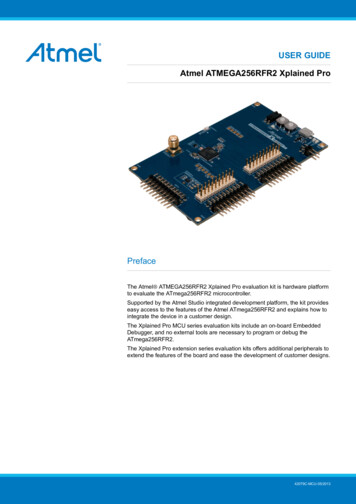
Figure 1-1. ATMEGA256RFR2 Xplained Pro evaluation kit overview.Atmel ATMEGA256RFR2 Xplained Pro [USER GUIDE]42079C-MCU-05/20134
2.Getting started2.1Quick-start3 Steps to start exploring the Atmel Xplained Pro Platform2.21 Download and install Atmel Studio . Launch Atmel Studio. Connect an USB cable to the DEBUG USB port.Connecting the kitWhen connecting Atmel ATMEGA256RFR2 Xplained Pro to your computer for the first time, the operatingsystem will do a driver software installation. The driver file supports both 32-bit and 64-bit versions ofMicrosoft Windows XP and Windows 7.Once connected the green power LED will be lit and Atmel Studio will autodetect which Xplained Proevaluation- and extension kit(s) that's connected. You'll be presented with relevant information like datasheetsand kit documentation. You also have the option to launch Atmel Software Framework (ASF) exampleapplications. The target device is programmed and debugged by the on-board Embedded Debugger and no2external programmer or debugger tool is needed. Please refer to the Atmel Studio user guide for informationregarding how to compile and program the kit.2.3Design documentation and related linksThe following list contains links to the most relevant documents and software for the ATMEGA256RFR2Xplained Pro.31.Xplained Pro products - Atmel Xplained Pro is a series of small-sized and easy-to-use evaluation kitsfor 8- and 32-bit Atmel microcontrollers. It consists of a series of low cost MCU boards for evaluation anddemonstration of features and capabilities of different MCU families.2.ATMEGA256RFR2 Xplained Pro User Guide - PDF version of this User Guide.3.ATMEGA256RFR2 Xplained Pro Design Documentation - Package containing schematics, BOM,assembly drawings, 3D plots, layer plots etc.4.Atmel Studio - Free Atmel IDE for development of C/C and assembler code for Atmelmicrocontrollers.5.IAR Embedded Workbench for Atmel AVR . This is a commercial C/C compiler that is availablefor 8-bit AVR. There is a 30 day evaluation version as well as a 4k code size limited kick-start versionavailable from their website.6.Atmel sample store - Atmel sample store where you can order samples of -ATMEGA256RFR2-Xplained-Pro 2079-ATMEGA256RFR2-Xplained-Pro tmel ATMEGA256RFR2 Xplained Pro [USER GUIDE]42079C-MCU-05/20135
3.Xplained ProXplained Pro is an evaluation platform that provides the full Atmel microcontroller experience. The platformconsists of a series of Microcontroller (MCU) boards and extension boards that are integrated with AtmelStudio, have Atmel Software Framework (ASF) drivers and demo code, support data streaming and more.Xplained Pro MCU boards support a wide range of Xplained Pro extension boards that are connected througha set of standardized headers and connectors. Each extension board has an identification (ID) chip to uniquelyidentify which boards are mounted on a Xplained Pro MCU board. This information is used to present relevantuser guides, application notes, datasheets and example code through Atmel Studio. Available Xplained Pro1MCU and extension boards can be purchased in the Atmel Web Store .3.1Embedded DebuggerThe ATMEGA256RFR2 Xplained Pro contains the Atmel Embedded Debugger (EDBG) for on-boarddebugging. The EDBG is a composite USB device of 3 interfaces; a debugger, Virtual COM Port and DataGateway Interface (DGI).In conjunction with Atmel Studio, the EDBG debugger interface can program and debug the ATmega256RFR2.On the ATMEGA256RFR2 Xplained Pro, the JTAG interface is connected between the EDBG and theATmega256RFR2.The Virtual COM Port is connected to a UART port on the ATmega256RFR2 (see section “EmbeddedDebugger implementation” on page 14 for pinout), and provides an easy way to communicate with the targetapplication through a simple terminal software. It offers variable baud rate, parity and stop bit settings. Notethat the settings on the target device UART must match the settings given in the terminal software.The DGI consists of several physical data interfaces for communication with the host computer. Please,see section “Embedded Debugger implementation” on page 14 for available interfaces and pinout.Communication over the interfaces are bidirectional. It can be used to send events and values from theATmega256RFR2, or as a generic printf-style data channel. Traffic over the interfaces can be timestampedon the EDBG for more accurate tracing of events. Note that timestamping imposes an overhead that reducesmaximal throughput. The DGI uses a proprietary protocol, and is thus only compatible with Atmel Studio.The EDBG controls two LEDs on ATMEGA256RFR2 Xplained Pro, a power LED and a status LED. Table 3-1,“EDBG LED control” shows how the LEDs are controlled in different operation modes.Table 3-1. EDBG LED controlOperation modePower LEDStatus LEDNormal operationPower LED is lit when power isapplied to the board.Activity indicator, LED flashesevery time something happens onthe EDBG.Bootloader mode (idle)The power LED and the status LED blinks simultaneously.Bootloader mode (firmwareupgrade)The power LED and the status LED blinks in an alternating pattern.For further documentation on the EDBG, see the EDBG User Guide.3.2Hardware identification systemAll Xplained Pro compatible extension boards have an Atmel ATSHA204 crypto authentication chip mounted.This chip contains information that identifies the extension with its name and some extra data. When anXplained Pro extension board is connected to an Xplained Pro MCU board the information is read and sentto Atmel Studio. The Atmel Kits extension, installed with Atmel Studio, will give relevant information, codeexamples and links to relevant documents. Table 3-2, “Xplained Pro ID chip content” shows the data fieldsstored in the ID chip with example content.Table 3-2. Xplained Pro ID chip content1Data FieldData TypeExample ContentManufacturerASCII stringAtmel’\0’Product NameASCII stringSegment LCD1 Xplained Pro’\0’Product RevisionASCII string02’\0’http://store.atmel.com/Atmel ATMEGA256RFR2 Xplained Pro [USER GUIDE]42079C-MCU-05/20136
3.3Data FieldData TypeExample ContentProduct Serial NumberASCII string1774020200000010’\0’Minimum Voltage [mV]uint16 t3000Maximum Voltage [mV]uint16 t3600Maximum Current [mA]uint16 t30Power supplyThe ATMEGA256RFR2 Xplained Pro kit can be powered either by USB or by an external power source throughthe 4-pin power header, marked PWR. This connector is described in “Power header” on page 8. Theavailable power sources and specifications are listed in Table 3-3, “Power sources for ATMEGA256RFR2Xplained Pro”.Table 3-3. Power sources for ATMEGA256RFR2 Xplained ProPower inputVoltage requirementsCurrent requirementsConnector markingExternal power4.3V to 5.5VRecommendedminimum is 500mAto be able to provideenough currentfor extentions andthe board itself.Recommendedmaximum is 2A dueto the input protectionmaximum currentspecification.PWREmbedded debuggerUSB4.4V to 5.25V(according to USB spec)500 mA (according toUSB spec)DEBUG USBThe kit will automatically detect which power sources are available and choose which one to use according tothe following priority:3.3.11.External power2.Embedded debugger USBMeasuring ATmega256RFR2 power consumptionAs part of an evaluation of the ATmega256RFR2 it can be of interest to measure its power consumption.Because the device has a separate power plane (VCC MCU P3V3) on this board it is possible to measure thecurrent consumption by measuring the current that is flowing into this plane. The VCC MCU P3V3 plane isconnected via a jumper to the main power plane (VCC TARGET P3V3) and by replacing the jumper with anampere meter it is possible to determine the current consumption. To locate the current measurement header,please refer to Figure 1-1, “ATMEGA256RFR2 Xplained Pro evaluation kit overview.”.WarningDo not power the board without having the jumper or an ampere meter mounted. This can causethe ATmega256RFR2 to be powered through its I/O pins and cause undefined operation of thedevice.3.4Standard headers and connectors3.4.1Xplained Pro extension headerAll Xplained Pro kits have one or more dual row, 20 pin, 100mil extension headers. Xplained Pro MCU boardshave male headers while Xplained Pro extensions have their female counterparts. Note that all pins arenot always connected. However, all the connected pins follow the defined pin-out described in Table 3-4,“Xplained Pro extension header”. The extension headers can be used to connect a wide variety of Xplained Proextensions to Xplained Pro MCU boards and to access the pins of the target MCU on Xplained Pro MCU boarddirectly.Atmel ATMEGA256RFR2 Xplained Pro [USER GUIDE]42079C-MCU-05/20137
Table 3-4. Xplained Pro extension headerPin numberNameDescription1IDCommunication line to the ID chip on extension board.2GNDGround3ADC( )Analog to digital converter , alternatively positive part of differentialADC4ADC(-)Analog to digital converter , alternatively negative part ofdifferential ADC5GPIO1General purpose IO6GPIO2General purpose IO7PWM( )Pulse width modulation , alternatively positive part of differentialPWM8PWM(-)Pulse width modulation , alternatively positive part of differentialPWM9IRQ/GPIOInterrupt request line and/or general purpose IO.10SPI SS B/GPIOSlave select for SPI and/or general purpose IO.11TWI SDAData line for two wire interface. Always implemented, bus type.12TWI SCLClock line for two wire interface. Always implemented, bus type.13USART RXReceiver line of Universal Synchronous and Asynchronous serialReceiver and Transmitter14USART TXTransmitter line of Universal Synchronous and Asynchronousserial Receiver and Transmitter15SPI SS ASlave select for SPI. Should be unique if possible.16SPI MOSIMaster out slave in line of Serial peripheral interface. Alwaysimplemented, bus type17SPI MISOMaster in slave out line of Serial peripheral interface. Alwaysimplemented, bus type18SPI SCKClock for Serial peripheral interface. Always implemented, bustype19GNDGround20VCCPower for extension board3.4.2Power headerThe power header can be used to connect external power to the ATMEGA256RFR2 Xplained Pro kit. Thekit will automatically detect and switch to the external power if supplied. The power header can also be usedas supply for external peripherals or extension boards. Care must be taken not to exceed the total currentlimitation of the on-board regulator for the 3.3V regulated output. To locate the current measurement header,please refer to Figure 1-1, “ATMEGA256RFR2 Xplained Pro evaluation kit overview.”Table 3-5. Power header PWRNotePin number PWR headerPin nameDescription1VEXT P5V0External 5V input2GNDGround3VCC P5V0Unregulated 5V (output, derivedfrom one of the input sources)4VCC P3V3Regulated 3.3V (output, used asmain power for the kit)If the board is powered from a battery source it is recommended to use the PWR header. If thereis a power source connected to EDBG USB, the EDBG is activated and it will consume morepower.Atmel ATMEGA256RFR2 Xplained Pro [USER GUIDE]42079C-MCU-05/20138
4.Hardware user guide4.1ConnectorsThis chapter describes the implementation of the relevant connectors and headers on ATMEGA256RFR2Xplained Pro and their connection to the ATmega256RFR2. The tables of connections in this chapter alsodescribes which signals are shared between the headers and on-board functionality.4.1.1I/O extension headersThe ATMEGA256RFR2 Xplained Pro headers EXT1, EXT2, EXT3, EXT4 and EXT5 offers access to the I/Oof the microcontroller in order to expand the board e.g. by connecting extension modules to the board. Theseheaders all comply with the standard extension header specified in Xplained Pro Standard Extension Header.All headers have a pitch of 2.54 mm.Table 4-1. Extension header EXT1Pin on EXT1ATmega256RFR2 pinFunction1Communication line toID chip on extensionboard.2GNDShared C1A8PB6OC1B9PE5GPIO / INT5EXT4 header.10PD5GPIO / SPI chip select BEXT4 header.11PD1TWI SDAAll EXT headers.12PD0TWI SCLAll EXT headers.13PE0UART0 RXDAll EXT headers.EXT2, EXT3 and EXT5connected through cutstrap.14PE1UART0 TXDAll EXT headers.EXT2, EXT3 and EXT5connected through cutstrap.15PG0GPIO / SPI chip select AEXT4 header.16PB2SPI MOSIAll EXT headers.17PB3SPI MISOAll EXT headers.18PB1SPI SCKAll EXT headers.19GND20VCCEXT4 header.Table 4-2. Extension header EXT2Pin on EXT2ATmega256RFR2 pinFunction1Communication line toID chip on extensionboard.2GNDShared functionalityAtmel ATMEGA256RFR2 Xplained Pro [USER GUIDE]42079C-MCU-05/20139
Pin on EXT2ATmega256RFR2 pinFunctionShared functionality9PE6GPIO / INT6EXT5 header.10PD6GPIO / SPI chip select BEXT5 header.11PD1TWI SDAAll other EXT headers.12PD0345678TWI SCLAll other EXT headers.UART0 RXDAll other EXT headers.EXT2, EXT3 and EXT5connected through cutstrap.UART0 TXDAll other EXT headers.EXT2, EXT3 and EXT5connected through cutstrap.13PE0114PE1115PD4GPIO / SPI chip select AEXT5 header.16PB2SPI MOSIAll other EXT headers.17PB3SPI MISOAll other EXT headers.18PB1SPI SCKAll other EXT headers.19GND20Notes:VCC1Connected through cut-strapTable 4-3. Extension header EXT3Pin on EXT3ATmega256RFR2 pinFunction1Communication line toID chip on extensionboard.2GNDShared functionality3PF3GPIO4PG5GPIO5PB7GPIO9PE7GPIO / INT710PD7GPIO / SPI chip select B11PD1TWI SDAAll other EXT headers.12PD067813PE0114PE11TWI SCLAll other EXT headers.UART0 RXDAll other EXT headers.EXT2, EXT3 and EXT5connected through cutstrap.UART0 TXDAll other EXT headers.EXT2, EXT3 and EXT5Atmel ATMEGA256RFR2 Xplained Pro [USER GUIDE]42079C-MCU-05/201310
Pin on EXT3ATmega256RFR2 pinFunction15PG4GPIO / SPI chip select A16PB2SPI MOSIAll other EXT headers.17PB3SPI MISOAll other EXT headers.18PB1SPI SCKAll other EXT headers.19GND20VCCNotes:Shared functionalityconnected through cutstrap.1Connected through cut-strapTable 4-4. Extension header EXT4Pin on EXT4ATmega256RFR2 pinFunction1Communication line toID chip on extensionboard.2GNDShared functionality34567PB5OC1AEXT1 header.9PE5GPIO / INT5EXT1 header.10PG0GPIO / SPI chip select BEXT1 header.11PD1TWI SDAAll other EXT headers.12PD0TWI SCLAll other EXT headers.13PE0UART0 RXDAll other EXT headers.EXT2, EXT3 and EXT5connected through cutstrap.14PE1UART0 TXDAll other EXT headers.EXT2, EXT3 and EXT5connected through cutstrap.15PD5GPIO / SPI chip select AEXT1 header.16PB2SPI MOSIAll other EXT headers.17PB3SPI MISOAll other EXT headers.18PB1SPI SCKAll other EXT headers.819GND20VCCTable 4-5. Extension header EXT5Pin on EXT5ATmega256RFR2 pinFunction1Communication line toID chip on extensionboard.2GNDShared functionality3Atmel ATMEGA256RFR2 Xplained Pro [USER GUIDE]42079C-MCU-05/201311
Pin on EXT5ATmega256RFR2 pinFunctionShared functionality9PE6GPIO / INT6EXT2 header.10PD4GPIO / SPI chip select BEXT2 header.11PD1TWI SDAAll other EXT headers.12PD045678All other EXT headers.UART0 RXDAll other EXT headers.EXT2, EXT3 and EXT5connected through cutstrap.UART0 TXDAll other EXT headers.EXT2, EXT3 and EXT5connected through cutstrap.13PE014PE1115PD6GPIO / SPI chip select AEXT2 header.16PB2SPI MOSIAll other EXT headers.17PB3SPI MISOAll other EXT headers.18PB1SPI SCKAll other EXT headers.19GND20Notes:4.1.2TWI SCL1VCC1Connected through cut-strapOther headersIn addition to the “I/O extension headers” on page 9, ATMEGA256RFR2 Xplained Pro has additionally twoheaders with spare signals which offers access to the I/O of the microcontroller which are otherwise not easilyavailable elsewhere or might be favourable to have collected toghether. All headers have a pitch of 2.54mm.Table 4-6. SPARE ADC signals headerPin on headerATmega256RFR2pinFunction1-VCC (3.3V)2PF4ADC43PF54PF65Notes:PF7Shared functionality1JTAG Interface, TCK1JTAG Interface, TMS1JTAG Interface, TDO1JTAG Interface, TDIADC5ADC6ADC71These lines are connected to the JTAG interface, and ADC will not work properly while debugging or programming the kit.Table 4-7. SPARE signals header 2Pin on headerATmega256RFR2pinFunction1AREFAnalog reference2TSTTest pin for RF testmode3RSTNReset4RSTONReset status5CLKIAlternative mainclock inputShared functionalityEDBG and RESET buttonAtmel ATMEGA256RFR2 Xplained Pro [USER GUIDE]42079C-MCU-05/201312
Pin on FunctionShared functionalityGNDThe ATMEGA256RFR2 Xplained Pro kit contains two crystals that can be used as clock sources for theATmega256RFR2 device. Each crystal has a cut-strap next to it that can be used to measure the oscillatorallowance. This is done by cutting the strap and adding a resistor across the strap. More information about1oscillator allowance and safety factor can be found in appnote AVR4100Table 4-8. External 32.768kHz crystalsPin on ATmega256RFR2FunctionPG3TOSC2, crystal outputPG4TOSC1, crystal inputTable 4-9. External 16MHz crystals4.2.2Pin on ATmega256RFR2FunctionXTAL1Crystal inputXTAL2Crystal outputMechanical buttonsATMEGA256RFR2 Xplained Pro contains two mechanical buttons. One button is the RESET button connectedto the ATmega256RFR2 reset line and the other is a generic user configurable button. When a button ispressed it will drive the I/O line to GND.Table 4-10. Mechanical buttons4.2.3Pin on ATmega256RFR2Silkscreen textRSTNRESETPE4SW0LEDThere is one yellow LED available on the ATMEGA256RFR2 Xplained Pro board that can be turned on and off.The LED can be activated by driving the connected I/O line to GND.Table 4-11. LED connections4.2.4Pin on ATmega256RFR2LEDPB4Yellow LEDRFThe main feature of ATMEGA256RFR2 Xplained Pro is to show the RF capability of the ATmega256RFR2device. This device has bidirectional differential antenna pins, which are fed through a balun (Johanson2Technology, 2450BM15A0015 ) to create a single unbalanced output/input. This kit has a passive analog RF3switch (Skyworks Solutions Inc, AS222-92LF ) connected to the unbalanced output of the balun. The switchis driven by the DIG1 and DIG2 pins of the ATmega256RFR2 which feature Antenna Diversity to enable thedevice to automatically select the best signal from two antennas (can also be selected manually). The output4of the switch is connected to a ceramic chip antenna (Johanson Technology, 2540AT18D0100 ) and a SMAconnector for external na 2450AT18D0100 v3.pdf23Atmel ATMEGA256RFR2 Xplained Pro [USER GUIDE]42079C-MCU-05/201313
Table 4-12. RF connectionsPin on ATmega256RFR24.2.5RFPRF balanced output (Positive)RFNRF balanced output (Negative)Temperature sensorATMEGA256RFR2 Xplained Pro features an Atmel AT30TSE758 temperature sensor chip with an 8kbitserial EEPROM inside. The sensor includes programmable high and low temperature alarms, user-selectabletemperature resolution up to 12 bits, and an I2C/SMBus compatible serial interface.Table 4-13. Temperature sensor connections.AT30TSE758temperaturesensor pinPin namePin onCommentATmega256RFR21SDAPD1Data line of serial interface2SCLPD0Clock line of serial interface13ALERTNC4GNDGND5A2-Addres line for serial interface, by default pulled low6A1-Addres line for serial interface, by default pulled high7A0-Addres line for serial interface, by default pulled highVCCVCC8Notes:Temperature alarm signalling pin1Alert pin is available on a testpoint hole close to the sensor.The temperature sensor has two TWI addresses, one for the temperature sensor and one for the EEPROM.The addresses are "0b1001 A2 A1 A0" for the temperature sensor and "0b1010 A2 A1 A0" for the EEPROM.The address selection lines (A2, A1 and A0) of the temperature sensor chip is by default pulled high for A0 andA1 and low for A2, through 100kΩ resistors, which makes the default addresses 0b1001011 and 0b1010011.Soldering the the straps on the front of the ATMEGA256RFR2 Xplained Pro board for An will alter that bit inthe address to low or high. Each strap is marked in silkscreen with A0, A1 and A2 as shown in Figure 4-1,“Temperature sensor TWI address.”. When communicating with the EEPROM, part of the TWI address is used5as a page address, for more details see the device datasheet .Figure 4-1. Temperature sensor TWI address.4.3Embedded Debugger implementationThe ATMEGA256RFR2 Xplained Pro contains an Embedded Debugger (EDBG) that can be used toprogram and debug the ATmega256RFR2 using JTAG. The Embedded Debugger also include a Virtual Comport interface over UART, an Atmel Data Gateway Interface over SPI and TWI and it monitors four of theATmega256RFR2 GPIOs. Atmel Studio can be used as a front end for the Embedded Debugger.4.3.1JTAGThe JTAG use five pins to communicate with the target. For further information on how to use the programmingand debugging capabilities of the EDBG, see “Embedded Debugger” on page 6.5http://www.atmel.com/Images/doc8751.pdfAtmel ATMEGA256RFR2 Xplained Pro [USER GUIDE]42079C-MCU-05/201314
Table 4-14. JTAG connections.4.3.2Pin on ATmega256RFR2FunctionPF4JTAG TCKPF5JTAG TMSPF6JTAG TDOPF7JTAG TDIRSTNRESETVirtual COM portThe Embedded Debugger act as a Virtual Com Port gateway by using one of the ATmega256RFR2 UARTs.For further information on how to use the Virtual COM port see “Embedded Debugger” on page 6.Table 4-15. Virtual COM port connections.4.3.3Pin on ATmega256RFR2FunctionPD2UART RXD (ATmega256RFR2 RX line)PD3UART TXD (ATmega256RFR2 TX line)Atmel Data Gateway InterfaceThe Embedded Debugger features an Atmel Data Gateway Interface (DGI) by using either a SPI or TWIport. The DGI can be used to send a variety of data from the ATmega256RFR2 to the host PC. For furtherinformation on how to use the DGI interface see “Embedded Debugger” on page 6.Table 4-16. DGI interface connections when using SPI.Pin on ATmega256RFR2FunctionPB0Slave select (ATmega256RFR2 is Master)PB1SPI SCK (Clock Out)PB2SPI MOSI (Master Out, Slave in)PB3SPI MISO (Master In, Slave Out)Table 4-17. DGI interface connections when using TWI.Pin on ATmega256RFR2FunctionPD0SCL (Clock line)PD1SDA (Data line)Four GPIO lines are connected to the Embedded Debugger. The EDBG can monitor these lines and timestamp pin value changes. This makes it possible to accurately time stamp events in the ATmega256RFR2application code. For further information on how to configure and use the GPIO monitoring features see“Embedded Debugger” on page 6.Table 4-18. GPIO lines connected to the EDBG.Pin on IO3Atmel ATMEGA256RFR2 Xplained Pro [USER GUIDE]42079C-MCU-05/201315
5.Agency Certification5.1UNITED STATES (FCC)This equipment complies with Part 15 of the FCC rules and regulations. To fulfill FCC Certificationrequirements, an OEM manufacturer must comply with the following regulations:1.ImportantThis equipment (ATMEGA256RFR2 Xplained Pro) is for use for evaluation purposes only and must not beincorporated into any other device or system.This equipment complies with Part 15 of the FCC Rules. Operation is subject to the following twoconditions: (1) this device may not cause harmful interference, and (2) this device must acceptany interference received, including interference that may cause undesired operation (FCC15.19).The internal / external antenna(s) used for this mobile transmitter must provide a separation distance of atleast 20 cm from all persons and must not be colocated or operating in conjunction with any other antenna ortransmitter.Installers must be provided with antenna installation instructions and transmitter operating conditions forsatisfying RF exposure compliance. This device is approved as a mobile device with respect to RF exposurecompliance, and may only be marketed to OEM installers. Use in portable exposure conditions (FCC 2.1093)requires separate equipment authorization.ImportantModifications not expressly approved by this company could void the user's authority to operatethis equipment (FCC section 15.21).ImportantThis equipment has been tested and found to comply with the limits for a Class A digital device,pursuant to Part 15 of the FCC Rules. These limits are designed to provide reasonable protectionagainst harmful interference when the equipment is operated in a commercial environment.This equipment generates, uses, and can radiate radio frequency energy and, if not installedand used in accordance with the instruction manual, may cause harmful interference to radiocommunications. Operation of this equipment in a residential a
The Atmel ATMEGA256RFR2 Xplained Pro evaluation kit is a hardware platform to evaluate the Atmel ATmega256RFR2. The kit offers a set of features that enables the ATmega256RFR2 user to get started using the ATmega256RFR2 peripherals right away and to get an understanding of how to integrate the device in their