Transcription
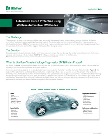
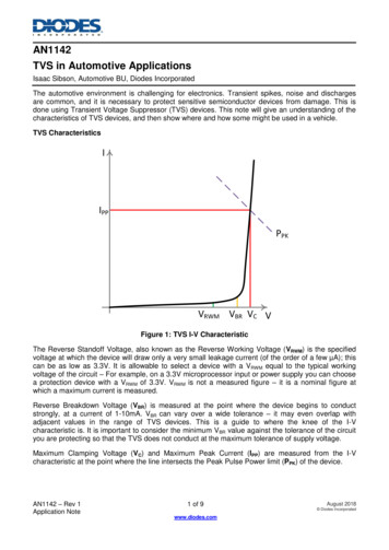
AN1142TVS in Automotive ApplicationsIsaac Sibson, Automotive BU, Diodes IncorporatedThe automotive environment is challenging for electronics. Transient spikes, noise and dischargesare common, and it is necessary to protect sensitive semiconductor devices from damage. This isdone using Transient Voltage Suppressor (TVS) devices. This note will give an understanding of thecharacteristics of TVS devices, and then show where and how some might be used in a vehicle.TVS CharacteristicsIIPPPPKVRWM VBR VC VFigure 1: TVS I-V CharacteristicThe Reverse Standoff Voltage, also known as the Reverse Working Voltage (VRWM) is the specifiedvoltage at which the device will draw only a very small leakage current (of the order of a few µA); thiscan be as low as 3.3V. It is allowable to select a device with a VRWM equal to the typical workingvoltage of the circuit – For example, on a 3.3V microprocessor input or power supply you can choosea protection device with a VRWM of 3.3V. VRWM is not a measured figure – it is a nominal figure atwhich a maximum current is measured.Reverse Breakdown Voltage (VBR) is measured at the point where the device begins to conductstrongly, at a current of 1-10mA. VBR can vary over a wide tolerance – it may even overlap withadjacent values in the range of TVS devices. This is a guide to where the knee of the I-Vcharacteristic is. It is important to consider the minimum VBR value against the tolerance of the circuityou are protecting so that the TVS does not conduct at the maximum tolerance of supply voltage.Maximum Clamping Voltage (VC) and Maximum Peak Current (IPP) are measured from the I-Vcharacteristic at the point where the line intersects the Peak Pulse Power limit (PPK) of the device.AN1142 – Rev 1Application Note1 of 9www.diodes.comAugust 2018 Diodes Incorporated
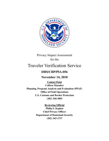
AN1142DirectionalityAn important aspect of TVS devices is directionality. The most basic type of TVS is unidirectional:ISingle Polarity ofcircuit operationVFigure 2: Unidirectional TVS device symbol and characteristicThis type of device is used where the operating area of the circuit to be protected is always positive,for example 0 to 5V. The device will protect against positive and negative transients (immediately,as forward conduction in the device).ICircuit operatespositive andnegativeVFigure 3: Bidirectional TVS device symbol and characteristicWhere the circuit has both positive and negative operation, such as a split rail audio system or adifferential signalling scheme, a bidirectional TVS provides protection for transients that go beyondthe safe operating area – either positive or negative.Bidirectional TVS can be either symmetrical (VBR is the same in both directions) or asymmetrical (VBRis greater in one direction than the other direction).AN1142 – Rev 1Application Note2 of 9www.diodes.comAugust 2018 Diodes Incorporated
AN1142Why are Reverse Standoff Voltage and Reverse Breakdown Voltage positive? ve circuit voltageVRWM, VBR and VC are positive, like the operating voltages of thecircuit being protected – the voltage that transients will be limited to.This is the convention used across the industry, even though thedevice is being used in the reverse direction.Reverse CurrentFlowFigure 4: Reverse current flowZener TVS compared to Zener DiodeOften the same symbols are used for Zener TVS devices as for Zener Diodes, and it may give rise toquestions about the differences between the two. Both devices rely on the Zener breakdown effectand have I-V characteristics that look very similar. What is the difference?IZenerDiodeTVSPTVSPZVZVRWM VBRVFigure 5: Zener and TVS I-V characteristics comparedAlthough they appear similar, a closer look at the I-V characteristics in Figure 5 immediately showsthe differences. The Zener Diode (blue trace, Vz) has a much sharper knee, steeper slope and tightervoltage tolerance (dashed lines and shaded region) than a TVS device.These differences come from design and optimization – the purpose of a Zener Diode is to provide anaccurate voltage clamp within a signal circuit, or as a reference or regulator. A Zener diode willnormally have current flowing through it either constantly or for longer periods of time (severalseconds in a clamp application) The TVS exists to handle the energy from spikes and transients thatmight otherwise cause damage to sensitive components. The TVS device is designed to absorb alarge amount of energy in a very short time (nanoseconds to milliseconds). The peak currents can bevery large but not for continuous operation. The accuracy of a TVS is less important than theaccuracy of a Zener Diode.During normal circuit operation the TVS device should not conduct other than leakage.AN1142 – Rev 1Application Note3 of 9www.diodes.comAugust 2018 Diodes Incorporated
AN1142Power RatingOn first inspection the power ratings of TVS devices seem extraordinarily high, but the power rating isa pulse rating. A TVS device is not intended for continuous operation.IIPP½ IPPt1tt2Figure 6: TVS Test PulseA typical pulse waveform is shown in Figure 6. Two common waveforms are used, with differentvalues of t1 and t2. Those waveforms are known as 8/20 (t1 8µs, t2 20µs, defined in IEC61000-45) and 10/1000 (t1 10µs, t2 1000µs, defined in IEC61643-321). Note that t2 is elapsed time from0, not t1.The 8/20 pulse shows how the device will handle events like ESD discharge and lightning strikes.The 10/1000 pulse shows how the device will handle slower speed higher energy events like powersupply surges. In automotive applications, these events are likely to come from the alternator andinductive loads.A TVS device may have two different power ratings, one relating to each of these pulses, and theyare quite different. It is much clearer why that is the case if the two pulses are overlaid to scale asshown in figure 7.I8/20 IPP10/1000 IPPtFigure 7: TVS 8/20 compared with 10/1000AN1142 – Rev 1Application Note4 of 9www.diodes.comAugust 2018 Diodes Incorporated
AN1142The published power figure is VC IPP. VC varies with IPP – therefore the lower IPP of the 10/1000pulse also gives a lower VC, again reducing the Peak Power figure.For the shorter time duration spike on the 8/20 pulse (Blue trace), the device can handle a muchhigher current. The important thing is the energy of the pulse, represented by the area under thecurve (shaded blue area, 0-20µs). Compare to the 10/1000 pulse (Orange trace) and it’s clear thatthe area under the curve (shaded orange area, 0-1000µs) is much greater, limiting the peak figure.The easiest way to think about this is that the device has an internal capacity to absorb a set amountof energy as heat. That can happen at very high rates for a very short time, or lower rates for a longertime.TVS Products in an Automotive SystemIn a vehicle there are several specific areas in which TVS devices might be used, protecting againstsomewhat different threats.SSTX /USBPortUSB3.1 SSRX /2 Hub3Regulator1ACANH/L1LoadDumpTVS3 12V212VBatteryECU/ ECM2 CANDevice3LIN32 LINDevice0VFigure 8: TVS Devices within an Automotive SystemThe 12V system of a traditional car is powered from the Alternator, and its output is rectified andregulated to provide the nominal 12V to charge the battery and provide power to accessories.Because both the generation and some of the loads (e.g. window motors, wiper motors, seat motors,etc.) are inductive, there can be significant spikes and dips on the 12V power system as loads areconnected, disconnected, stall, etc. Of course, cranking and ignition of an Internal CombustionEngine also presents a very significant and difficult load. This rail also experiences ESD dischargesand noise from many systems like ignition coils, injectors and HID lamps.To protect the systems within the vehicle there are multiple levels of TVS devices. There are verylarge TVS devices fitted around the alternator and regulator (marked 1 in figure 10) to absorb highenergy events like load dump, field decay, etc.Each electronic module attached to the 12V power will have its own TVS (marked 2 in figure 10) andreverse polarity protection. The data buses that connect these various modules are not directlyvulnerable to the power rail threats, but they will be liable to pick up noise and ESD discharges, whichconnect to the relatively sensitive low-voltage microprocessors. These buses have protection devicesalso (marked 3 in figure 10).AN1142 – Rev 1Application Note5 of 9www.diodes.comAugust 2018 Diodes Incorporated
AN1142Automotive Power Rail PulsesThe standards ISO 7637-2 and ISO 16750 set out a series of defined pulses on the 12V power railthat must be dealt with by the system. Figure 9 gives a sense of these pulses – their magnitude andwhat they are meant to model. (Note: not to scale)Pulse 1VPulse 3100VPulse 2Pulse 487VPulse 5aSupply Disconnectfrom inductive load12V200ms100ns50V40 - 400ms0.5 – 20s50µsDisconnectof parallelloadLoad DumptSwitching spikesICE Cranking-75V-150VFigure 9: Automotive test pulsesIt is important to consider the system as a whole – for example, there may be a main Load DumpTVS which is very large and placed close to the alternator. This will absorb most of the energy in aload dump event, and for this reason there is an option to test automotive modules with the remainingload dump energy that would reach them:V87VPulse 5aPulse 5btFigure 10: Pulse 5a compared with Pulse 5bThe magnitude of pulse 5b is determined by the customer, by defining the voltage of the main loaddump TVS.AN1142 – Rev 1Application Note6 of 9www.diodes.comAugust 2018 Diodes Incorporated
AN1142Pulses 1 and 5 in Figure 9 have a significantly longer time duration than the 10/1000µs test pulsedescribed on page 4. TVS products in automotive applications therefore will require greater powerhandling than those in a non-automotive environment.Power Rail TVSECU/ ECMFigure 11: TVS power rail device within an automotive moduleEach module within a vehicle will tend to have both reverse battery polarity protection (shown here asa diode, but often implemented as a MOSFET) and a TVS device to protect that module fromtransients. A TVS device fitted to the power input of an ECU must be rugged and capable ofdissipating a significant energy, although it will not be trying to handle the entire energy of a loaddump event, for example. Industry-standard devices such as SMCJ28C/CAQ, packaged in the 1.5kW(10/1000µs) rated SMC package, are typically deployed to protect powerlines.However, the drive toward high-power dissipation and reduced footprint has resulted in thedevelopment of TVS in the small form factor thermally efficient PowerDI 5 package. TheD28V0HU12P5Q is the first TVS to be packaged in the thermally efficient PowerDI 5 package. Thedevice features a reverse stand-off voltage of 28V and low reverse leakage while being able todissipate up to 1800W of power per 10/1000s transient, which is 20% higher than comparable SMCsolutions while occupying just 40% of the PCB area.CAN bus and FlexRayCAN NodeCAN Node0VFigure 12: CAN bus TVS protection deviceModern vehicles carry a lot of data over buses such as CAN and FlexRay. These buses can carrysafety-critical information so they must not only be rugged but also reliable. It is important that thesebuses are protected from transients and noise and are protected in a way that does not reduce thebandwidth of the signal. These buses are more likely to encounter low-energy noise and ESD thanhigh-energy transients like load dump. For this reason, smaller, lower power protection devices areappropriate.CAN bus and FlexRay are differential buses, and so they require dual bidirectional TVS to protectboth of the data lines. They should be low capacitance to maintain signal integrity.CAN bus is not necessarily ground referenced – different nodes in the vehicle may experiencedifferent ground voltages. The TVS device can limit both common and differential mode spikes toprotect the CAN devices.AN1142 – Rev 1Application Note7 of 9www.diodes.comAugust 2018 Diodes Incorporated
AN1142LIN busSignal: 24/-15V rangeLINSlaveLIN Master0VFigure 13: LIN bus TVS protection deviceIn simple physical terms the LIN bus is a 2 wire bus comprising of signal and ground wires. Thesignal can potentially be between 24V and -15V (due to ground level variance around a vehicle), soan asymmetrical bidirectional device is required.The Diodes Inc. DESD1CAN2S0Q and DESD1FLEX2S0Q are dual bidirectional parts suitable forCAN and FlexRay respectively. The DESD1LIN2WSQ is a compact 2-terminal asymmetric TVSdevice suited to LIN applications.PartApplicationVRWM (V)VBR(min) (V)VBR(max) (V)VC (V) @ 3AIPP 525.4/17.127.8/18.950/353SOD323USB/DataUSB and high-speed data buses like HDMI may also require TVS protection. These connectionshave multiple lines and run at high speed, so low capacitance is key to preserve data integrity. Formultiple data lines small packaging is critical to fit multiple devices into limited board area.SSTX SSTX-USB 3.1 PortUSB ControllerSSRX SSRX-D5V0F2U3LPQD5V0F2U3LPQ0V0VFigure 14: USB 3.1 data line protection TVS deviceFor high-speed data applications, devices such as the D5V0F2U3LPQ offer low capacitance tomaintain signal integrity. The small X-DFN1006-3 package allows dual devices to be fitted into lessboard space – ideal for high speed data pairs in USB 3.1.PowerDI is a Registered Trademark of Diodes IncorporatedAN1142 – Rev 1Application Note8 of 9www.diodes.comAugust 2018 Diodes Incorporated
AN1142IMPORTANT NOTICEDIODES INCORPORATED MAKES NO WARRANTY OF ANY KIND, EXPRESS OR IMPLIED, WITH REGARDS TO THIS DOCUMENT,INCLUDING, BUT NOT LIMITED TO, THE IMPLIED WARRANTIES OF MERCHANTABILITY AND FITNESS FOR A PARTICULARPURPOSE (AND THEIR EQUIVALENTS UNDER THE LAWS OF ANY JURISDICTION).Diodes Incorporated and its subsidiaries reserve the right to make modifications, enhancements, improvements, corrections or otherchanges without further notice to this document and any product described herein. Diodes Incorporated does not assume any liabilityarising out of the application or use of this document or any product described herein; neither does Diodes Incorporated convey any licenseunder its patent or trademark rights, nor the rights of others. Any Customer or user of this document or products described herein in suchapplications shall assume all risks of such use and will agree to hold Diodes Incorporated and all the companies whose products arerepresented on Diodes Incorporated website, harmless against all damages.Diodes Incorporated does not warrant or accept any liability whatsoever in respect of any products purchased through unauthorized saleschannel.Should Customers purchase or use Diodes Incorporated products for any unintended or unauthorized application, Customers shallindemnify and hold Diodes Incorporated and its representatives harmless against all claims, damages, expenses, and attorney fees arisingout of, directly or indirectly, any claim of personal injury or death associated with such unintended or unauthorized application.Products described herein may be covered by one or more United States, international or foreign patents pending. Product names andmarkings noted herein may also be covered by one or more United States, international or foreign trademarks.This document is written in English but may be translated into multiple languages for reference. Only the English version of this documentis the final and determinative format released by Diodes Incorporated.LIFE SUPPORTDiodes Incorporated products are specifically not authorized for use as critical components in life support devices or systems without theexpress written approval of the Chief Executive Officer of Diodes Incorporated. As used herein:A. Life support devices or systems are devices or systems which:1. are intended to implant into the body, or2. support or sustain life and whose failure to perform when properly used in accordance with instructions for use provided in thelabeling can be reasonably expected to result in significant injury to the user.B. A critical component is any component in a life support device or system whose failure to perform can be reasonably expected to causethefailure of the life support device or to affect its safety or effectiveness.Customers represent that they have all necessary expertise in the safety and regulatory ramifications of their life support devices orsystems, and acknowledge and agree that they are solely responsible for all legal, regulatory and safety-related requirements concerningtheir products and any use of Diodes Incorporated products in such safety-critical, life support devices or systems, notwithstanding anydevices- or systems-related information or support that may be provided by Diodes Incorporated. Further, Customers must fully indemnifyDiodes Incorporated and its representatives against any damages arising out of the use of Diodes Incorporated products in such safetycritical, life support devices or systems.Copyright 2018, Diodes Incorporatedwww.diodes.comAN1142 – Rev 1Application Note9 of 9www.diodes.comAugust 2018 Diodes Incorporated
The 10/1000 pulse shows how the device will handle slower speed higher energy events like power supply surges. In automotive applications, these events are likely to come from the alternator and inductive loads. A TVS device may have two different power ratings, one relating to each of these pulses, and they are quite different.