Transcription
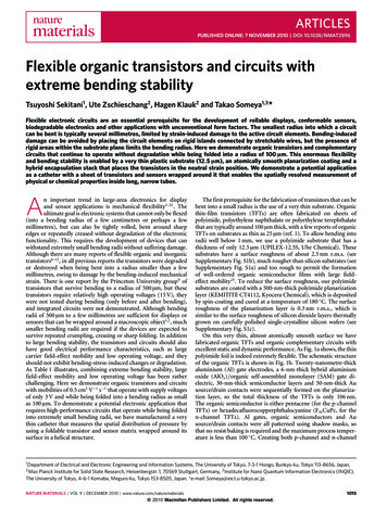
ARTICLESPUBLISHED ONLINE: 7 NOVEMBER 2010 DOI: 10.1038/NMAT2896Flexible organic transistors and circuits withextreme bending stabilityTsuyoshi Sekitani1 , Ute Zschieschang2 , Hagen Klauk2 and Takao Someya1,3 *Flexible electronic circuits are an essential prerequisite for the development of rollable displays, conformable sensors,biodegradable electronics and other applications with unconventional form factors. The smallest radius into which a circuitcan be bent is typically several millimetres, limited by strain-induced damage to the active circuit elements. Bending-induceddamage can be avoided by placing the circuit elements on rigid islands connected by stretchable wires, but the presence ofrigid areas within the substrate plane limits the bending radius. Here we demonstrate organic transistors and complementarycircuits that continue to operate without degradation while being folded into a radius of 100 µm. This enormous flexibilityand bending stability is enabled by a very thin plastic substrate (12.5 µm), an atomically smooth planarization coating and ahybrid encapsulation stack that places the transistors in the neutral strain position. We demonstrate a potential applicationas a catheter with a sheet of transistors and sensors wrapped around it that enables the spatially resolved measurement ofphysical or chemical properties inside long, narrow tubes.An important trend in large-area electronics for displayand sensor applications is mechanical flexibility1–22 . Theultimate goal is electronic systems that cannot only be flexed(into a bending radius of a few centimetres or perhaps a fewmillimetres), but can also be tightly rolled, bent around sharpedges or repeatedly creased without degradation of the electronicfunctionality. This requires the development of devices that canwithstand extremely small bending radii without suffering damage.Although there are many reports of flexible organic and inorganictransistors6–12 , in all previous reports the transistors were degradedor destroyed when being bent into a radius smaller than a fewmillimetres, owing to damage by the bending-induced mechanicalstrain. There is one report by the Princeton University group9 oftransistors that survive bending to a radius of 500 µm, but thesetransistors require relatively high operating voltages (15 V), theywere not tested during bending (only before and after bending),and integrated circuits were not demonstrated. Although bendingradii of 500 µm to a few millimetres are sufficient for displays orsensors that can be wrapped around a macroscopic object1,2 , muchsmaller bending radii are required if the devices are expected tosurvive repeated crumpling, creasing or sharp folding. In additionto large bending stability, the transistors and circuits should alsohave good electrical performance characteristics, such as largecarrier field-effect mobility and low operating voltage, and theyshould not exhibit bending-stress-induced changes or degradation.As Table 1 illustrates, combining extreme bending stability, largefield-effect mobility and low operating voltage has been ratherchallenging. Here we demonstrate organic transistors and circuitswith mobilities of 0.5 cm2 V 1 s 1 that operate with supply voltagesof only 3 V and while being folded into a bending radius as smallas 100 µm. To demonstrate a potential electronic application thatrequires high-performance circuits that operate while being foldedinto extremely small bending radii, we have manufactured a verythin catheter that measures the spatial distribution of pressure byusing a foldable transistor and sensor matrix wrapped around itssurface in a helical structure.The first prerequisite for the fabrication of transistors that can bebent into a small radius is the use of a very thin substrate. Organicthin-film transistors (TFTs) are often fabricated on sheets ofpolyimide, polyethylene naphthalate or polyethylene terephthalatethat are typically around 100 µm thick, with a few reports of organicTFTs on substrates as thin as 25 µm (ref. 1). To allow bending intoradii well below 1 mm, we use a polyimide substrate that has athickness of only 12.5 µm (UPILEX-12.5S, Ube Chemical). Thesesubstrates have a surface roughness of about 2.5 nm r.m.s. (seeSupplementary Fig. S1b), much rougher than silicon substrates (seeSupplementary Fig. S1a) and too rough to permit the formationof well-ordered organic semiconductor films with large fieldeffect mobility23 . To reduce the surface roughness, our polyimidesubstrates are coated with a 500-nm-thick polyimide planarizationlayer (KEMITITE CT4112, Kyocera Chemical), which is depositedby spin-coating and cured at a temperature of 180 C. The surfaceroughness of the planarization layer is 0.3 nm r.m.s., which issimilar to the surface roughness of silicon dioxide layers thermallygrown on carefully polished single-crystalline silicon wafers (seeSupplementary Fig. S1c).On this very thin, almost atomically smooth surface we havefabricated organic TFTs and organic complementary circuits withexcellent static and dynamic performance. As Fig. 1a shows, the thinpolyimide foil is indeed extremely flexible. The schematic structureof the organic TFTs is shown in Fig. 1b. Twenty-nanometre-thickaluminium (Al) gate electrodes, a 6-nm-thick hybrid aluminiumoxide (AlOx )/organic self-assembled monolayer (SAM) gate dielectric, 30-nm-thick semiconductor layers and 50-nm-thick Ausource/drain contacts were sequentially formed on the planarization layer, so the total thickness of the TFTs is only 106 nm.The organic semiconductor is either pentacene (for the p-channelTFTs) or hexadecafluorocopperphthalocyanine (F16 CuPc, for then-channel TFTs). Al gates, organic semiconductors and Ausource/drain contacts were all patterned using shadow masks, sothat no resist baking is required and the maximum process temperature is less than 100 C. Creating both p-channel and n-channel1 Departmentof Electrical and Electronic Engineering and Information Systems, The University of Tokyo, 7-3-1 Hongo, Bunkyo-ku, Tokyo 113-8656, Japan,Planck Institute for Solid State Research, Heisenbergstr. 1, 70569 Stuttgart, Germany, 3 Institute for Nano Quantum Information Electronics (INQIE),The University of Tokyo, 4-6-1 Komaba, Meguro-ku, Tokyo 153-8505, Japan. *e-mail: Someya@ee.t.u-tokyo.ac.jp.2 MaxNATURE MATERIALS VOL 9 DECEMBER 2010 www.nature.com/naturematerials 2010 Macmillan Publishers Limited. All rights reserved.1015
NATURE MATERIALS DOI: 10.1038/NMAT2896ARTICLESTable 1 Comparison with literature data.Field-effect mobilityOperating voltageMinimum bending radiusPolycrystallinesilicon TFTs(ref. 6)Metal oxideTFTs(ref. 7)Amorphoussilicon TFTs(refs 8,9)Organic TFTs(ref. 10)Organic TFTs(ref. 12)Organic TFTs(this work) 10 cm2 V 1 s 14V10 mm7 cm2 V 1 s 110 V30 mm0.5 cm2 V 1 s 115 V0.5 mm0.5 cm2 V 1 s 140 V0.5 mm0.1 cm2 V 1 s 12.5 V2.5 mm0.5 cm2 V 1 s 12V0.1 mmCarrier field-effect mobility, operating voltage and bending stability reported for inorganic and organic TFTs.abSource and drain contacts (Au)OrganicsemiconductorSAMPlanarization layer(polyimide)Polyimide substrateGate electrode (Al)cPentaceneSAM (2 nm)AlOx(4 nm)Al (18 nm)Polyimide(planarization layer)20 nmdTubeCircuit2 mmAu electrodeCatheterPressure-sensitive rubberFigure 1 Ultraflexible integrated circuits. a, Photographs of a 12.5-µm-thick polyimide substrate with functional organic TFTs and organic complementarycircuits. The array has an area of 75 75 mm2 . b, Schematic cross-section of the TFTs. c, High-resolution cross-sectional electron microscopy image of aflexible TFT. The specimen was prepared using a focused ion beam and imaged by transmission electron microscopy (300 kV). d, Photograph of a thincatheter that measures the spatial distribution of pressure along its length and circumference by means of an active-matrix sensor helix. A cross-sectionalillustration of the development view is also shown.TFTs allows for the design of complementary circuits, which havesubstantially smaller power consumption, larger gain and greaternoise immunity than unipolar circuits24–26 .The final process step is the deposition of a hybrid encapsulationstack that serves two purposes. As the encapsulation stack iscomposed of a metal layer (Au, 200 nm thick) sandwiched betweentwo polymer layers (parylene, 300 nm and 12.5 µm thick), it is1016an excellent barrier against the diffusion of oxygen and humidityfrom the ambient air into the organic semiconductors, and hencegreatly increases the air stability of the devices and circuits27 .Moreover, as the encapsulation stack has the same thickness asthe polyimide substrate (that is, 13 µm), the TFTs and circuitsare now located in the neutral strain position (where bendinginduced compressive and tensile strain cancel each other), whichNATURE MATERIALS VOL 9 DECEMBER 2010 www.nature.com/naturematerials 2010 Macmillan Publishers Limited. All rights reserved.
NATURE MATERIALS DOI: 10.1038/NMAT2896ARTICLESaCurrent density (A cm 2)10 3Al/AlOx/SAM/Au capacitors(area: 700 100 µm2)10 5Polyimide substrate10 710 9Si/SiO2 substrate10 11 3 2 10Voltage (V)bcDrain current (A)Drain current (µA)100 1.5 1.0 0.5Drain source voltage (V)FFFCuNF10 1010 1110 11 2.5 2.0 1.5 1.0 0.5Gate source voltage (V)FF10 1210 6VDS 2 VF0FNNN10 7FFN Cu NFFFFFFFF10 1010 7NNN10 9F40200.51.01.5Drain source voltage (V)2.010 8NNNFFF10 8FFF10 910 910 1010 1010 1110 1110 12 1.0 0.500.51.0Gate source voltage (V)1.5Gate current (A)F10 9FNNN10 8FFN10 810 6Drain current (A)F10 7FF80Drain current (nA)eVGS 1 to 1.5 V10 710 12 3010 6VDS 2 VGate current (A)0 2.0010 510 5 0.40310 6 0.8602VGS 1 to 2 V 1.2d110 122.0Figure 2 Performance of organic TFTs on plastic substrates. a, Leakage current through the 6-nm-thick AlOx /SAM gate dielectric as a function ofapplied voltage. Measurements were carried out on Al/AlOx /SAM/Au capacitors on two different substrates: a 12.5-µm-thick polyimide substrate with a500-nm-thick polyimide planarization layer (red curve), and a thermally oxidized, single-crystalline silicon wafer (blue curve). b, Drain current as afunction of drain–source voltage for a pentacene p-channel TFT (gate–source voltage (VGS ) in steps of 0.5 V). c, Drain current and gate current as afunction of gate–source voltage for a pentacene p-channel TFT (drain–source voltage (VDS ): 2 V). Owing to the small thickness of the gate dielectric(6 nm), the operation voltage is about 2 V. The field-effect mobility extracted from the transfer characteristics is 0.5 cm2 V 1 s 1 . d, Drain current as afunction of drain–source voltage for a F16 CuPc n-channel TFT (gate–source voltage in steps of 0.5 V). e, Drain current and gate current as a function ofgate–source voltage for a F16 CuPc n-channel TFT (drain–source voltage: 2 V). The mobility is 0.01 cm2 V 1 s 1 . Hysteresis and gate leakage are very smallfor both types of TFT.NATURE MATERIALS VOL 9 DECEMBER 2010 www.nature.com/naturematerials 2010 Macmillan Publishers Limited. All rights reserved.1017
NATURE MATERIALS DOI: 10.1038/NMAT2896ARTICLESaCurrent strain(perpendicular)Current strain(parallel)GSGSCapacitorDD700 100 (μm)W/L 500/50 (μm)13-μm-thick mide13-μm-thick polyimide substratebc1.210 80.8Gate current (A)Normalized drain current1.0Current strain0.6Current strainCurrent strain10 9Current strain10 100.40.20101.00.1Bending radius (mm)0.0110 11101.00.1Bending radius (mm)0.01Figure 3 Bending tests on ultraflexible organic TFTs. a, Photographs of a TFT in which the drain current flows parallel to the bending-induced strain, of aTFT in which the current flows perpendicularly to the strain and of an Al/AlOx /SAM/Au capacitor that allows measurement of the gate dielectriccapacitance during bending. The TFTs have a channel length of 50 µm and a channel width of 500 µm. The capacitor has an area of 700 100 µm2 .Bending was carried out using a custom-built precision bending apparatus. b, Measured drain currents of two pentacene TFTs (red: strain parallel to thedrain current; blue: strain perpendicular to the drain current) as a function of bending radius during inward bending, normalized to the initial drain currentmeasured in the flat state. c, Gate currents of the same TFTs measured during inward bending. Drain–source voltage: 2 V; gate–source voltage: 2.5 V.means they are not subjected to strain and thus are highly stableduring sharp bending9,10 .Figure 1c shows a high-resolution cross-sectional electronmicroscopy image of a completed transistor. The specimen wasprepared using a focused ion beam (FB-2100, Hitachi HighTechnologies) and imaged by transmission electron microscopy(HF-3300 Cold-FE TEM, 300 kV, Hitachi High-Technologies). The1018Al gate as well as the 4-nm-thick AlOx layer and the 2-nmthick SAM of the hybrid gate dielectric is clearly resolved in thetransmission electron micrograph. Owing to the small surfaceroughness provided by the 500-nm-thick polyimide planarizationlayer, the individual TFT layers are very smooth. When theplanarization layer is omitted, the TFT layers are much rougher (seeSupplementary Fig. S2b).NATURE MATERIALS VOL 9 DECEMBER 2010 www.nature.com/naturematerials 2010 Macmillan Publishers Limited. All rights reserved.
NATURE MATERIALS DOI: 10.1038/NMAT2896ARTICLESabVDDOutput voltage N1.52.040FFNCuNF1 mm0.5FF30GainF0Input voltage (V)FFR 300 μm0.5n-channel TFTFR (initial)1.5F10FF200F01.00.5Input voltage (V)cVDD4R (initial)R 300 μmOutput voltage (V)321VDD 3 V004080120160Time (ms)1 mmFigure 4 Ultraflexible organic circuits. a, Photograph of a polyimide substrate with functional organic TFTs and circuits wrapped around a cylinder with aradius of 300 µm. b, Circuit diagram, photograph and electrical transfer characteristics of a complementary inverter (composed of a pentacene p-channelTFT and a F16 CuPc n-channel TFT) operated with a supply voltage (VDD ) of 2 V. The TFTs have a channel length of 20 µm. The transfer characteristics weremeasured in the flat state and while the inverter was bent into a radius of 300 µm. There is no discernible change in characteristics during bending.c, Circuit diagram, photograph and output signals of a five-stage complementary ring oscillator operated with a supply voltage (VDD ) of 3 V in the flat stateand while bent into a radius of 300 µm. The circuit oscillates with a signal delay per stage of 4.5 ms, both in the flat state and during tight bending.NATURE MATERIALS VOL 9 DECEMBER 2010 www.nature.com/naturematerials 2010 Macmillan Publishers Limited. All rights reserved.1019
NATURE MATERIALS DOI: 10.1038/NMAT2896ARTICLESbaGate source voltagePressuresensitiverubber(sensor)Drain source voltagecd10 5VDS 3 V10 61 kPaDrain current (A)10 710 810 910 100 kPa10 1110 12 3.0 2.5 2.0 1.5 1.0Gate source voltage (V) 0.50Figure 5 Tightly wound pressure-sensor helix. a, Circuit diagram of an ultraflexible active-matrix pressure-sensor array in the shape of a tightly woundhelix. b, Photographs of a TFT array fabricated on a shape-memory polymer film (NIPPON MEKTRON, Japan) and permanently transformed into a helix.Even when the helix is stretched by 50% the TFTs remain functional. c, Photograph of a tightly wound active-matrix sensor array for a catheter thatmeasures the spatial distribution of pressure. The array was fabricated by laminating three sheets: (1) a foldable 4 36 array of pentacene TFTs, (2) apressure-sensitive rubber sheet and (3) a 12.5- µm-thick polyimide sheet with a Au counter electrode. d, Transfer characteristics of an individual sensorcell measured at two different pressures. (Note that applying pressure to the pressure-sensitive rubber sheet creates a conducting path between thesource of the TFT and the counter electrode. Thus, the potential of 3 V is present on the source of the TFT only when pressure is applied, allowing thearray to measure the spatial distribution of pressure.)Despite the small gate dielectric thickness (6 nm), the leakagecurrents through the dielectric are below 10 5 A cm 2 at an applied voltage of 3 V (which corresponds to an electric field of5 MV cm 1 ; see Fig. 2a). The current–voltage characteristics of apentacene p-channel and a F16 CuPc n-channel TFT fabricated ona substrate with a 500-nm-thick polyimide planarization layer areshown in Fig. 2b–e. The mobilities (0.5 cm2 V 1 s 1 for pentacene,0.01 cm2 V 1 s 1 for F16 CuPc), subthreshold swings and on/offratios are essentially identical to those of TFTs on glass25 , and thehysteresis in the transfer curves (Fig. 2c,e) is negligible. The electrical characteristics are stable during exposure to air for six months,which is a direct result of the excellent gas barrier characteristics ofthe 13-µm-thick parylene/Au/parylene passivation stack27 .To confirm the critical role of the 500-nm-thick polyimideplanarization layer for achieving good device performance, wehave also fabricated TFTs on a polyimide substrate without aplanarization layer. The lack of a planarization layer leads to amuch greater surface roughness of the Al gate electrodes and theAlOx /SAM gate dielectric (see Supplementary Figs S1 and S2b), so1020the pentacene films in these transistors are characterized by muchsmaller field-effect mobility (0.01 cm2 V 1 s 1 ) and substantialhysteresis (see Supplementary Fig. S3).The bending stability of the transistors was evaluated by bendingthe substrate into a radius as small as 100 µm along an axis runningexactly through the TFTs, with the direction of the bending-inducedstrain aligned either parallel or perpendicularly to the directionof the current flow from drain to source (see Fig. 3a). Bendingwas carried out using a custom-built bending apparatus, and theelectrical characteristics were measured while the devices were beingbent (see Supplementary Fig. S4). Figure 3b shows the measureddrain currents of two pentacene TFTs (one bent in the paralleldirection and one bent in the perpendicular direction) as a functionof bending radius, normalized to the drain current measured in theflat state. Figure 3c shows the gate currents of the same TFTs foreach bending radius. Supplementary Fig. S5 shows the capacitanceof an Al/AlOx /SAM/Au capacitor as a function of bending radius.As can be seen, the electrical characteristics of the TFTs are stable forbending radii down to 100 µm, which is by far the smallest bendingNATURE MATERIALS VOL 9 DECEMBER 2010 www.nature.com/naturematerials 2010 Macmillan Publishers Limited. All rights reserved.
NATURE MATERIALS DOI: 10.1038/NMAT2896radius reported for an organic (or inorganic) field-effect transistor.Comparing Fig. 3b and c suggests that the damage that occurs whenthe bending radius is decreased below 100 µm originates in the gatedielectric of the transistors.For comparison, we have also carried out bending tests on pentacene TFTs fabricated on thicker polyimide substrates (thickness75 µm instead of 12.5 µm) and fabricated without the 13-µm-thickparylene/Au/parylene encapsulation stack. In this case, the TFTs arenot located in the neutral strain position and thus are fully exposedto the bending-induced mechanical strain. The measurement results, shown in Supplementary Fig. S6, indicate that in these TFTsdamage occurs at a much larger bending radius ( 3.5 mm), whichconfirms the benefit of employing an encapsulation stack that placesthe TFTs in the neutral strain position.We have also evaluated the bending stability of organiccomplementary inverters and ring oscillators fabricated along withthe pentacene p-channel and F16 CuPc n-channel TFTs on theflexible polyimide substrates. There are only very few reportsof flexible organic complementary ring oscillators, and in allof them the circuits either required large operating voltages28,29or had to be operated in an inert environment owing to theuse of semiconductors with air degradation30 . Figure 4a shows aphotograph of a 12.5-µm-thick polyimide substrate (complete witha 500-nm-thick planarization layer, organic devices and circuits,and a 13-µm-thick encapsulation stack) tightly wrapped arounda cylinder with a radius of 300 µm. Figure 4b shows the circuitdiagram, a photograph and the static transfer characteristics of acomplementary inverter (composed of a pentacene p-channel TFTand a F16 CuPc n-channel TFT) fabricated on this substrate. Thetransfer characteristics were measured in ambient air in the flatstate and while the substrate was bent into a radius of 300 µm.There is no discernible change in the electrical characteristicsduring bending. The schematic, a photograph and the outputsignal of a five-stage complementary ring oscillator operated witha supply voltage of 3 V are shown in Fig. 4c. The signal delay atthis supply voltage is 4.5 ms per stage, similar to circuits madeon glass25 . The signal delays in the range of a few millisecondsare fast enough for certain sensor applications such as artificialskins2 , as highlighted in Figs 1 and 5. Furthermore, as can beseen, the circuit continues to oscillate in the bent state, andthe output signal is unaffected by bending of the ring oscillatorinto a radius of 300 µm. The circuits shown in Fig. 4 werefabricated on a polyimide substrate and therefore relax back intothe flat state when released from the cylinder around whichthey had been wrapped.An interesting option we have also explored is the fabrication ofcircuits on a shape-memory polymer film31 . The substrate is initiallyin its flat state to facilitate fabrication of high-performance organicdevices. After wrapping the substrate around a cylinder into a helix,it is heated to a temperature of about 150 C and then allowed tocool, which causes the substrate to permanently adapt the helicalstructure, as shown in Fig. 5b.To demonstrate a possible application for organic TFTs thatoperate in the bent state, we have manufactured a thin catheter thatmeasures the spatial distribution of mechanical pressure. The sensorwas fabricated by laminating three sheets: a foldable 4 36 array ofpentacene TFTs, a pressure-sensitive rubber sheet and a 12.5- µmthick polyimide sheet with a gold counter electrode. The pictureis shown in Fig. 1d and demonstrated in Fig. 5 and SupplementaryFig. S9. The source contacts of all 144 transistors are connected tothe rubber sheet, and the counter electrode is in contact with theopposite surface of the rubber sheet. When mechanical pressureis exerted on the catheter, the electrical resistance between therubber’s top and bottom surfaces decreases (see SupplementaryFig. S9). A potential of 3 V applied to the counter electrode issupplied to the TFTs in those positions where pressure is applied,ARTICLESand thus the spatial distribution of pressure can be obtained byinterrogating the TFTs in the active-matrix array.We have demonstrated that low-voltage organic transistors thatare fabricated on planarized polymeric substrate and covered withan encapsulation stack that places the devices into the neutralstrain position operate reliably and with excellent performancecharacteristics while being folded into a bending radius as small as100 µm. This may open a wide range of opportunities for electronicapplications that require a high degree of mechanical flexibilitycombined with operating voltages accessible by small batteries. Asan example we have illustrated a thin catheter that measures thespatial distribution of mechanical pressure using a helical sensorarray enabled by ultraflexible organic transistors.Received 25 May 2010; accepted 8 October 2010;published online 7 November 2010References1. Huitema, H. E. A., Gelinck, G. H., van Lieshout, P. J. G., van Veenendaal, E.& Touwslager, F. J. Flexible electronic-paper active-matrix displays.J. Soc. Inf. Display 14, 729–733 (2006).2. Someya, T. et al. Conformable, flexible, large-area networks ofpressure and thermal sensors with organic transistor active matrixes.Proc. Natl Acad. Sci. USA 102, 12321–12325 (2005).3. Bettinger, C. J. & Bao, Z. Organic thin-film transistors fabricated on resorbablebiomaterial substrates. Adv. Mater. 22, 651–655 (2010).4. Siegel, A. C. et al. Printable electronics: Foldable printed circuit boards onpaper substrates. Adv. Funct. Mater. 20, 28–35 (2010).5. Ko, H. C. et al. A hemispherical electronic eye camera based on compressiblesilicon optoelectronics. Nature 454, 748–753 (2008).6. Kodaira, T. et al. A flexible 2.1-in. active-matrix electrophoretic displaywith high resolution and a thickness of 100 µm. J. Soc. Inf. Displays 16,107–111 (2008).7. Nomura, K. et al. Room-temperature fabrication of transparent flexiblethin-film transistors using amorphous oxide semiconductors. Nature 432,488–492 (2004).8. Gleskova, H., Wagner, S., Soboyejo, W. & Suo, Z. Electrical response ofamorphous silicon thin-film transistors under mechanical strain. J. Appl. Phys.92, 6224–6229 (2002).9. Han, L., Song, K., Mandlik, P. & Wagner, S. Ultraflexible amorphous silicontransistors made with a resilient insulator. Appl. Phys. Lett. 96, 042111 (2010).10. Sekitani, T. et al. Ultraflexible organic field-effect transistors embedded at aneutral strain position. Appl. Phys. Lett. 87, 173502 (2005).11. Roberts, M. E. et al. Cross-linked polymer gate dielectric films for low-voltageorganic transistors. Chem. Mater. 21, 2292–2299 (2009).12. Jedaa, A. & Halik, M. Toward strain resistant flexible organic thin filmtransistors. Appl. Phys. Lett. 95, 103309 (2009).13. Sekitani, T. et al. Stretchable active-matrix organic light-emitting diode displayusing printable elastic conductors. Nature Mater. 8, 494–499 (2009).14. Ishida, K. et al. Stretchable EMI measurement sheet with 8 8 coil array,2 V organic CMOS decoder, and 0.18 µm silicon CMOS LSIs for electric andmagnetic field detection. IEEE J. Solid State Circ. 45, 249–259 (2010).15. Majewski, L. A., Schroeder, R., Voigt, M. & Grell, M. High performance organictransistors on cheap, commercial substrates. J. Phys. D 37, 3367–3372 (2004).16. Yoon, M. H., Facchetti, A. & Marks, T. J. σ –π molecular dielectric multilayersfor low-voltage organic thin-film transistors. Proc. Natl Acad. Sci. USA 102,4678–4682 (2005).17. Jang, Y. et al. Patterning the organic electrodes of all-organic thin filmtransistors with a simple spray printing technique. Appl. Phys. Lett. 89,183501 (2006).18. Kim, C. et al. Printable cross-linked polymer blend dielectrics. Design strategies,synthesis, microstructures, and electrical properties, with organic field-effecttransistors as testbeds. J. Am. Chem. Soc. 130, 6867–6878 (2008).19. Tan, H. S. et al. Solution-processed trilayer inorganic dielectric for highperformance flexible organic field effect transistors. Appl. Phys. Lett. 93,183503 (2008).20. Cai, Q. J. et al. Solution-processable barium titanate and strontium titanatenanoparticle dielectrics for low-voltage organic thin-film transistors.Chem. Mater. 21, 3153–3161 (2009).21. Zhang, X. H., Potscavage, W. J. Jr, Choi, S. & Kippelen, B. Low-voltage flexibleorganic complementary inverters with high noise margin and high dc gain.Appl. Phys. Lett. 94, 043312 (2009).22. Zschieschang, U. et al. Flexible low-voltage organic transistors and circuitsbased on a high-mobility organic semiconductor with good air stability.Adv. Mater. 22, 982–985 (2010).23. Lee, W. H. & Wang, C. C. Effect of nanocomposite gate dielectric roughness onpentacene field-effect transistor. J. Vac. Sci. Technol. B 27, 1116–1121 (2009).NATURE MATERIALS VOL 9 DECEMBER 2010 www.nature.com/naturematerials 2010 Macmillan Publishers Limited. All rights reserved.1021
NATURE MATERIALS DOI: 10.1038/NMAT2896ARTICLES24. Crone, B. K. et al. Design and fabrication of organic complementary circuits.J. Appl. Phys. 89, 5125–5132 (2001).25. Klauk, H., Zschieschang, U., Pflaum, J. & Halik, M. Ultralow-power organiccomplementary circuits. Nature 445, 745–748 (2007).26. Bode, D. et al. Noise-margin analysis for organic thin-film complementarytechnology. IEEE Trans. Electr. Dev. 57, 201–208 (2010).27. Sekitani, T & Someya, T. Air-stable operation of organic field-effecttransistors on plastic films using organic/metallic hybrid passivation layers.Jpn J. Appl. Phys. 46, 4300–4305 (2007).28. Klauk, H. et al. Flexible organic complementary circuits. IEEE Trans. Electr. Dev.52, 618–622 (2005).29. Yan, H. et al. Solution processed top-gate n-channel transistors andcomplementary circuits on plastics operating in ambient conditions.Adv. Mater. 20, 3393–3398 (2008).30. Na, J. H., Kitamura, M. & Arakawa, Y. Low-voltage-operating organiccomplementary circuits based on pentacene and C60 transistors. Thin Solid Films517, 2079–2082 (2009).31. Behl, M. & Lendlein, A. Actively moving polymers. Soft Matter 3, 58–67 (2007).1022AcknowledgementsThis study was partially supported by JST/CREST, the Grant-in-Aid for ScientificResearch (KAKENHI; WAKATE S), NEDO and the Special Coordination Funds forPromoting and Technology. We also thank S. Takatani for technical support anddiscussion, Athene for manufacturing very fine shadow masks, Daisankasei forhigh-purity parylene (diX-SR), and NIPPON MEKTRON, Japan for supplying athree-dimensional forming substrate as a shape-memory polymer film.Author contributionsT. Sekitani and T. Someya designed the concept. T. Sekitani, U.Z., H.K. and T. Someyacarried out experimental work, data analysis and wrote the paper. T. Someya supervisedthe project.Additional informationThe authors declare no competing financial interests. Supplementary informationaccompanies this paper on www.nature.com/naturematerials. Reprints and permissionsinformation is available online at spondence and requests for materials should be addressed to T. Someya.NATURE MATERIALS VOL 9 DECEMBER 2010 www.nature.com/naturematerials 2010 Macmillan Publishers Limited. All rights reserved.
SUPPLEMENTARY INFORMATIO
Figure 1 jUltraflexible integrated circuits. a, Photographs of a 12:5- m-thick polyimide substrate with functional organic TFTs and organic complementary circuits. The array has an area of 75 275mm . b, Schematic cross-section of the TFTs. c, High-resolution cross-sectional electron microscopy image of a flexible TFT.