Transcription
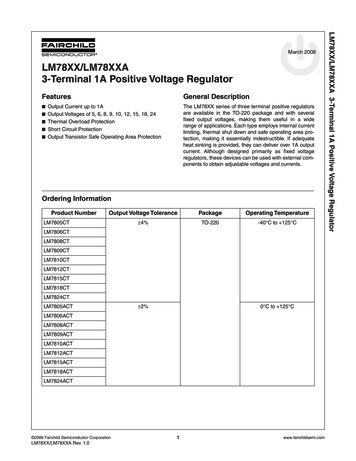
LM78XX/LM78XXA3-Terminal 1A Positive Voltage RegulatorFeaturesGeneral Description Output Current up to 1AThe LM78XX series of three terminal positive regulatorsare available in the TO-220 package and with severalfixed output voltages, making them useful in a widerange of applications. Each type employs internal currentlimiting, thermal shut down and safe operating area protection, making it essentially indestructible. If adequateheat sinking is provided, they can deliver over 1A outputcurrent. Although designed primarily as fixed voltageregulators, these devices can be used with external components to obtain adjustable voltages and currents. Output Voltages of 5, 6, 8, 9, 10, 12, 15, 18, 24 Thermal Overload Protection Short Circuit Protection Output Transistor Safe Operating Area ProtectionOrdering InformationProduct NumberOutput Voltage TolerancePackageOperating Temperature 4%TO-220-40 C to 125 M7815CTLM7818CTLM7824CTLM7805ACT 2%0 C to 125 15ACTLM7818ACTLM7824ACT 2006 Fairchild Semiconductor CorporationLM78XX/LM78XXA Rev. 1.01www.fairchildsemi.comLM78XX/LM78XXA 3-Terminal 1A Positive Voltage RegulatorMarch 2008
LM78XX/LM78XXA 3-Terminal 1A Positive Voltage RegulatorBlock DiagramInputSeries ProtectionGND2Figure 1.Pin AssignmentTO-220GND1. Input2. GND3. Output1Figure 2.Absolute Maximum RatingsAbsolute maximum ratings are those values beyond which damage to the device may occur. The datasheetspecifications should be met, without exception, to ensure that the system design is reliable over its power supply,temperature, and output/input loading variables. Fairchild does not recommend operation outside datasheetspecifications.SymbolVIParameterInput VoltageValueUnitVO 5V to 18V35VVO 24V40VRθJCThermal Resistance Junction-Cases (TO-220)5 C/WRθJAThermal Resistance Junction-Air (TO-220)65 C/WTOPROperating TemperatureRange-40 to 125 CTSTGLM78xxLM78xxAStorage Temperature Range-65 to 1502LM78XX/LM78XXA Rev. 1.00 to 125 Cwww.fairchildsemi.com
Refer to the test circuits. -40 C TJ 125 C, IO 500mA, VI 10V, CI 0.1µF, unless otherwise TJ 25 C4.85.05.2V5mA IO 1A, PO 15W,VI 7V to 20V4.755.05.25VO 7V to 25V–4.0100VI 8V to 12V–1.650.0IO 5mA to 1.5A–9.0100IO 250mA to 750mA–4.050.0–5.08.0mAQuiescent Current Change IO 5mA to 1A–0.030.5mAVI 7V to 25V–0.31.3IO 5mA–-0.8–mV/ Cf 10Hz to 100kHz, TA 25 C–42.0–µV/VO62.073.0–dBIO 1A, TJ 25 C–2.0–Vf 1kHz–15.0–mΩVI 35V, TA 25 C–230–mATJ 25 C–2.2–AOutput VoltageLine Regulation(1)Regload LoadIQ IQ VO/ TVNRRVDROPRegulation(1)Quiescent CurrentOutput VoltageDrift(2)Output Noise VoltageRippleRejection(2)Dropout VoltageResistance(2)rOOutputISCShort Circuit CurrentIPK(2)Peak CurrentConditionsTJ 25 CTJ 25 CTJ 25 Cf 120Hz, VO 8V to 18VmVmVNotes:1. Load and line regulation are specified at constant junction temperature. Changes in VO due to heating effects mustbe taken into account separately. Pulse testing with low duty is used.2. These parameters, although guaranteed, are not 100% tested in production.3LM78XX/LM78XXA Rev. 1.0www.fairchildsemi.comLM78XX/LM78XXA 3-Terminal 1A Positive Voltage RegulatorElectrical Characteristics (LM7805)
Refer to the test circuits. -40 C TJ 125 C, IO 500mA, VI 11V, CI 0.33µF, CO 0.1µF, unless otherwise sOutput VoltageLine Regulation(3)MinTyp.Max.UnitTJ 25 C5.756.06.25V5mA IO 1A, PO 15W,VI 8.0V to 21V5.76.06.3VI 8V to 25V–5.0120VI 9V to 13V–1.560.0IO 5mA to 1.5A–9.0120IO 250mA to 750mA–3.060.0TJ 25 C(3)Load RegulationTJ 25 CmVmVIQQuiescent CurrentTJ 25 C–5.08.0mA IQQuiescent CurrentChangeIO 5mA to 1A––0.5mAVI 8V to 25V––1.3Output Voltage DriftIO 5mA–-0.8–mV/ COutput Noise Voltagef 10Hz to 100kHz, TA 25 C–45.0–µV/VO62.073.0–dBIO 1A, TJ 25 C–2.0–Vf 1kHz–19.0–mΩVI 35V, TA 25 C–250–mATJ 25 C–2.2–A VO/ TVNRRVDROP(4)RippleRejection(4)Dropout VoltageResistance(4)rOOutputISCShort Circuit CurrentIPKCurrent(4)Peakf 120Hz, VO 8V to 18VNotes:3. Load and line regulation are specified at constant junction temperature. Changes in VO due to heating effects mustbe taken into account separately. Pulse testing with low duty is used.4. These parameters, although guaranteed, are not 100% tested in production.4LM78XX/LM78XXA Rev. 1.0www.fairchildsemi.comLM78XX/LM78XXA 3-Terminal 1A Positive Voltage RegulatorElectrical Characteristics (LM7806) (Continued)
Refer to the test circuits. -40 C TJ 125 C, IO 500mA, VI 14V, CI 0.33µF, CO 0.1µF, unless otherwise specified.SymbolVOReglineParameterOutput VoltageLine Regulation(5)(5)Regload Load RegulationIQ IQ VO/ TVNRRVDROPConditionsMin.Typ.Max.UnitTJ 25 C7.78.08.3V5mA IO 1A, PO 15W,VI 10.5V to 23V7.68.08.4VI 10.5V to 25V–5.0160VI 11.5V to 17V–2.080.0IO 5mA to 1.5A–10.0160IO 250mA to 750mA–5.080.0TJ 25 CTJ 25 CmVmVQuiescent CurrentTJ 25 C–5.08.0mAQuiescent Current ChangeIO 5mA to 1A–0.050.5mAVI 10.5V to 25V–0.51.0IO 5mA–-0.8–mV/ Cf 10Hz to 100kHz, TA 25 C–52.0–µV/VOf 120Hz, VO 11.5V to 21.5V56.073.0–dBIO 1A, TJ 25 C–2.0–Vf 1kHz–17.0–mΩVI 35V, TA 25 C–230–mATJ 25 C–2.2–AOutput VoltageDrift(6)Output Noise VoltageRippleRejection(6)Dropout VoltageResistance(6)rOOutputISCShort Circuit CurrentIPKCurrent(6)PeakNotes:5. Load and line regulation are specified at constant junction temperature. Changes in VO due to heating effects mustbe taken into account separately. Pulse testing with low duty is used.6. These parameters, although guaranteed, are not 100% tested in production.5LM78XX/LM78XXA Rev. 1.0www.fairchildsemi.comLM78XX/LM78XXA 3-Terminal 1A Positive Voltage RegulatorElectrical Characteristics (LM7808) (Continued)
Refer to the test circuits. -40 C TJ 125 C, IO 500mA, VI 15V, CI 0.33µF, CO 0.1µF, unless otherwise specified.SymbolVOReglineParameterOutput VoltageLine Regulation(7)ConditionsMin.Typ.Max.UnitTJ 25 C8.659.09.35V5mA IO 1A, PO 15W,VI 11.5V to 0–5.08.0mA––0.5mAVI 11.5V to 26V––1.3IO 5mA–-1.0–mV/ Cf 10Hz to 100kHz, TA 25 C–58.0–µV/VO56.071.0–dBIO 1A, TJ 25 C–2.0–Vf 1kHz–17.0–mΩVI 35V, TA 25 C–250–mATJ 25 C–2.2–ATJ 25 C VI 11.5V to 25VVI 12V to 17V(7)Regload Load RegulationTJ 25 C IO 5mA to 1.5AIO 250mA to 750mAIQ IQ VO/ TVNRRVDROPQuiescent CurrentTJ 25 CQuiescent Current Change IO 5mA to 1AOutput VoltageDrift(8)Output Noise VoltageRippleRejection(8)Dropout VoltageResistance(8)rOOutputISCShort Circuit CurrentIPKCurrent(8)Peakf 120Hz, VO 13V to 23VmVmVNotes:7. Load and line regulation are specified at constant junction temperature. Changes in VO due to heating effects mustbe taken into account separately. Pulse testing with low duty is used.8. These parameters, although guaranteed, are not 100% tested in production.6LM78XX/LM78XXA Rev. 1.0www.fairchildsemi.comLM78XX/LM78XXA 3-Terminal 1A Positive Voltage RegulatorElectrical Characteristics (LM7809) (Continued)
Refer to the test circuits. -40 C TJ 125 C, IO 500mA, VI 16V, CI 0.33µF, CO 0.1µF, unless otherwise specified.SymbolMin.Typ.Max.UnitTJ 25 C9.610.010.4V5mA IO 1A, PO 15W,VI 12.5V to 25V9.510.010.5VI 12.5V to 25V–10.0200VI 13V to 25V–3.0100IO 5mA to 1.5A–12.0200IO 250mA to 750mA–4.0400–5.18.0mA––0.5mAVI 12.5V to 29V––1.0Output Voltage Drift(10)IO 5mA–-1.0–mV/ CVNOutput Noise Voltagef 10Hz to 100kHz, TA 25 C–58.0–µV/VORRRipple Rejection(10)f 120Hz, VO 13V to 23V56.071.0–dBDropout VoltageIO 1A, TJ 25 C–2.0–VrOOutput Resistance(10)f 1kHz–17.0–mΩISCShort Circuit CurrentVI 35V, TA 25 C–250–mAIPKPeak Current(10)TJ 25 C–2.2–AVOReglineParameterOutput VoltageLine Regulation(9)Regload Load Regulation(9)IQ IQ VO/ TVDROPQuiescent CurrentConditionsTJ 25 CTJ 25 CTJ 25 CQuiescent Current Change IO 5mA to 1AmVmVNotes:9. Load and line regulation are specified at constant junction temperature. Changes in VO due to heating effects mustbe taken into account separately. Pulse testing with low duty is used.10. These parameters, although guaranteed, are not 100% tested in production.7LM78XX/LM78XXA Rev. 1.0www.fairchildsemi.comLM78XX/LM78XXA 3-Terminal 1A Positive Voltage RegulatorElectrical Characteristics (LM7810) (Continued)
Refer to the test circuits. -40 C TJ 125 C, IO 500mA, VI 19V, CI 0.33µF, CO 0.1µF, unless otherwise specified.SymbolVOReglineParameterOutput VoltageLine Regulation(11)ConditionsMin.Typ.Max.UnitTJ 25 C11.512.012.5V5mA IO 1A, PO 15W,VI 14.5V to 120–5.18.0mA–0.10.5mAVI 14.5V to 30V–0.51.0IO 5mA–-1.0–mV/ Cf 10Hz to 100kHz, TA 25 C–76.0–µV/VO55.071.0–dBIO 1A, TJ 25 C–2.0–Vf 1kHz–18.0–mΩVI 35V, TA 25 C–230–mATJ 25 C–2.2–ATJ 25 C VI 14.5V to 30VVI 16V to 22VRegload(11)Load RegulationTJ 25 C IO 5mA to 1.5AIO 250mA to 750mAIQ IQ VO/ TVNRRVDROPQuiescent CurrentQuiescent Current Change IO 5mA to 1AOutput VoltageDrift(12)Output Noise VoltageRippleRejection(12)Dropout VoltageResistance(12)rOOutputISCShort Circuit CurrentIPKTJ 25 CPeakCurrent(12)f 120Hz, VI 15V to 25VmVmVNotes:11. Load and line regulation are specified at constant junction temperature. Changes in VO due to heating effects mustbe taken into account separately. Pulse testing with low duty is used.12. These parameters, although guaranteed, are not 100% tested in production.8LM78XX/LM78XXA Rev. 1.0www.fairchildsemi.comLM78XX/LM78XXA 3-Terminal 1A Positive Voltage RegulatorElectrical Characteristics (LM7812) (Continued)
Refer to the test circuits. -40 C TJ 125 C, IO 500mA, VI 23V, CI 0.33µF, CO 0.1µF, unless otherwise specified.SymbolVOReglineParameterOutput VoltageLine Regulation(13)ConditionsMin.Typ.Max.UnitTJ 25 C14.415.015.6V5mA IO 1A, PO 15W,VI 17.5V to .0150–5.28.0mA––0.5mAVI 17.5V to 30V––1.0IO 5mA–-1.0–mV/ Cf 10Hz to 100kHz, TA 25 C–90.0–µV/VOf 120Hz, VI 18.5V to 28.5V54.070.0–dBIO 1A, TJ 25 C–2.0–Vf 1kHz–19.0–mΩVI 35V, TA 25 C–250–mATJ 25 C–2.2–ATJ 25 C VI 17.5V to 30VVI 20V to 26V(13)Regload Load RegulationTJ 25 C IO 5mA to 1.5AIO 250mA to 750mAIQ IQ VO/ TVNRRVDROPQuiescent CurrentQuiescent Current Change IO 5mA to 1AOutput VoltageDrift(14)Output Noise VoltageRippleRejection(14)Dropout VoltageResistance(14)rOOutputISCShort Circuit CurrentIPKTJ 25 CPeakCurrent(14)mVmVNotes:13. Load and line regulation are specified at constant junction temperature. Changes in VO due to heating effects mustbe taken into account separately. Pulse testing with low duty is used.14. These parameters, although guaranteed, are not 100% tested in production.9LM78XX/LM78XXA Rev. 1.0www.fairchildsemi.comLM78XX/LM78XXA 3-Terminal 1A Positive Voltage RegulatorElectrical Characteristics (LM7815) (Continued)
Refer to the test circuits. -40 C TJ 125 C, IO 500mA, VI 27V, CI 0.33µF, CO 0.1µF, unless otherwise TJ 25 C17.318.018.7V5mA IO 1A, PO 15W,VI 21V to 33V17.118.018.9TJ 25 C VI 21V to 33V–15.0360VI 24V to t Current Change IO 5mA to 1A––0.5mAVI 21V to 33V––1.0IO 5mA–-1.0–mV/ Cf 10Hz to 100kHz, TA 25 C–110–µV/VO53.069.0–dBIO 1A, TJ 25 C–2.0–Vf 1kHz–22.0–mΩVI 35V, TA 25 C–250–mATJ 25 C–2.2–AOutput VoltageLine Regulation(15)(15)Regload Load RegulationConditionsTJ 25 C IO 5mA to 1.5AIO 250mA to 750mAIQ IQ VO/ TVNRRVDROPQuiescent CurrentOutput VoltageDrift(16)Output Noise VoltageRippleRejection(16)Dropout VoltageResistance(16)rOOutputISCShort Circuit CurrentIPKPeakCurrent(16)TJ 25 Cf 120Hz, VI 22V to 32VmVmVNotes:15. Load and line regulation are specified at constant junction temperature. Changes in VO due to heating effects mustbe taken into account separately. Pulse testing with low duty is used.16. These parameters, although guaranteed, are not 100% tested in production.10LM78XX/LM78XXA Rev. 1.0www.fairchildsemi.comLM78XX/LM78XXA 3-Terminal 1A Positive Voltage RegulatorElectrical Characteristics (LM7818) (Continued)
Refer to the test circuits. -40 C TJ 125 C, IO 500mA, VI 33V, CI 0.33µF, CO 0.1µF, unless otherwise TJ 25 C23.024.025.0V5mA IO 1A, PO 15W,VI 27V to 38V22.824.025.25VI 27V to 38V–17.0480VI 30V to 36V–6.0240IO 5mA to 1.5A–15.0480IO 250mA to 750mA–5.0240–5.28.0mAQuiescent Current Change IO 5mA to 1A–0.10.5mAVI 27V to 38V–0.51.0IO 5mA–-1.5–mV/ Cf 10Hz to 100kHz, TA 25 C–60.0–µV/VO50.067.0–dBIO 1A, TJ 25 C–2.0–VOutput VoltageLine Regulation(17)(17)Regload Load RegulationIQ IQ VO/ TVNRRVDROPQuiescent CurrentOutput VoltageTJ 25 CTJ 25 CTJ 25 CDrift(18)Output Noise VoltageRippleConditionsRejection(18)Dropout Voltage(18)f 120Hz, VI 28V to 38VmVmVrOOutput Resistancef 1kHz–28.0–mΩISCShort Circuit CurrentVI 35V, TA 25 C–230–mATJ 25 C–2.2–AIPKPeakCurrent(18)Notes:17. Load and line regulation are specified at constant junction temperature. Changes in VO due to heating effects mustbe taken into account separately. Pulse testing with low duty is used.18. These parameters, although guaranteed, are not 100% tested in production.11LM78XX/LM78XXA Rev. 1.0www.fairchildsemi.comLM78XX/LM78XXA 3-Terminal 1A Positive Voltage RegulatorElectrical Characteristics (LM7824) (Continued)
SymbolVOReglineParameterOutput VoltageLine Regulation(19)ConditionsMin.Typ.Max.UnitTJ 25 C4.95.05.1VIO 5mA to 1A, PO 15W,VI 7.5V to 20V4.85.05.2VI 7.5V to 25V, IO 500mA–5.050.0VI
5 www.fairchildsemi.com LM78XX/LM78XXA Rev. 1.0 LM78XX/LM78XXA 3-Terminal 1A Positive Voltage Regulator Electrical Characteristics (LM7808) (Continued) Refer to the test circuits. -40 C TJ 125 C, IO 500mA, VI 14V, CI 0.33µF, CO 0.1µF, unless otherwise specified. Notes:
