Transcription
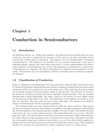
Chapter 1Conduction in Semiconductors1.1IntroductionAll solid-state devices, e.g. diodes and transistors, are fabricated from materials known as semiconductors. In order to understand the operation of these devices, the basic mechanism of howcurrents flow in them must be understood. This chapter covers the fundamentals of conductionin semiconductors. The chapter is not intended to be an extensive introduction to the area ofsolid-state physics. Instead, only those topics which lead to a better understanding of the macroscopic properties of semiconductors are covered. The mechanisms of conduction in a metal and ina semiconductor are compared. The effects of impurities on conduction in semiconductors are discussed. The formation of a p-n semiconductor junction is described and its conduction propertiesare discussed.1.2Classification of ConductorsFigure 1.1 illustrates a two-dimensional view of an atom that is called the Bohr model of the atom.It consists of a positively charged nucleus and a system of negatively charged electrons which rotatesaround the nucleus. In a neutral atom, the total charge is zero. This means that the positive chargeon the nucleus is equal to the total negative charge on the electrons. The electrons are bound tothe nucleus by the forces of attraction between oppositely charged particles. They are arrangedsystematically in layers called shells. The closer a shell is to the nucleus, the more tightly boundare the electrons in that shell to the atom. The shell closest to the nucleus can contain no morethan two electrons. The outer shell can have no more than eight. The number in the shells inbetween is determined by the laws of quantum mechanics.The outermost shell in an atom contains what are called the valence electrons. These governthe nature of chemical reactions of the elements. In addition, they play a large part in determiningthe electrical behavior of the elements and the crystalline structure of solids. The metallic elementstend to have one, two, or three valence electrons. The nonmetals have five, six, or seven. The inertgases have eight. The class of elements which have four valence electrons is called semiconductors.If a valence electron escapes its parent atom, it becomes free to move about. The parent atom thenhas a net positive charge and is called an ionized atom or an ion. If an electric field is applied to amaterial, the free electrons have forces exerted on them which cause them to move. This constitutesthe flow of a current in the material that is called a conduction current or a drift current.1
2CHAPTER 1. CONDUCTION IN SEMICONDUCTORSFigure 1.1: Two-dimensional Bohr model of an atom showing the nucleus and three shells.Depending on the number n of free electrons per unit volume in a solid, the material is classifiedas being a good conductor, a semiconductor, or an insulator. For a good conductor, n is very largeand is independent of temperature. A typical value is n ' 1028 per m3 . For an insulator at ordinarytemperatures, n is much smaller and has a typical value n ' 107 per m3 . For a semiconductor, itlies between the values for a good conductor and an insulator and is a function of the temperature.Silicon is an important semiconductor for which n ' 1.5 1016 per m3 at room temperature(T 300 K).1.3Conduction in MetalsMetals are classified as good conductors. The valence electrons are so loosely bound to the atomsthat they are free to move about in the conductor. Fig. 1.2 shows a two-dimensional illustration ofthe atoms in a metal with the free electrons distributed randomly among the immobile ions. Thefree electrons can be visualized as molecules of a gas that permeate the region between the ions.Analogous to the random motion of molecules in a gas, thermal energy causes the free electronsto be in continuous random motion. Observation of an individual electron would reveal that itsdirection of motion changes randomly after each collision with an ion. Because the direction ofmotion of each electron is random, the average number of electrons passing through any area perunit time is zero. Thus the average current flow in the metal is zero.1.3.1Drift Velocity If an electric field E ( V/ m) is applied to a metal, an electrostatic force is exerted on the freeelectrons which causes a conduction current to flow. (The arrow indicates a vector quantity.) The force on an individual electron is given by F q E ( N), where q is the electronic charge(q 1.602 10 19 C). The electrostatic forces cause the electrons to be accelerated in a directionopposite to that of the applied field. Fig. 1.3 illustrates the path that an individual electron mighttake under the influence of the electric field. If the electron did not collide with the bound ions, itsvelocity would increase indefinitely. However, energy is lost with each collision so that the average
1.3. CONDUCTION IN METALS3Figure 1.2: Two-dimensional view of the atoms in a metal with free electrons distributed randomlyamong the ions. velocity approaches a constant or steady-state value. The average velocity v ( m/ s) is called thedrift velocity. It is proportional to the applied field and is given by v µe E(1.1)where µe ( m2 V 1 s 1 ) is the electron mobility. (The minus sign is required because the negativecharge on the electron causes it to move is a direction opposite to the field.) The average distancethat the electron travels between collisions with the bound ions is called the mean free path. Asthe temperature increases, the bound ions vibrate with increasing intensity, causing the mean free path between collisions to decrease. This effect causes the drift velocity v to decrease, which ismodeled by a decrease in the electron mobility µe with temperature.Figure 1.3: Path taken by a free electron in a metal under the influence of an applied electric field.1.3.2Charge DensityThe charge density ρ ( C/ m3 ) in a conductor is defined as the free charge per unit volume. Torelate the charge density in a metal to the density of free electrons, let n be the number of electrons
4CHAPTER 1. CONDUCTION IN SEMICONDUCTORSper m3 . Because the charge per electron is q, it follows that the free charge per unit volume inthe metal is given byρ nq(1.2)1.3.3Current Density The current density J ( A/ m2 ) in a conductor is defined as the current per unit area flowing in aparticular direction. To relate the current density in a conductor to the drift velocity of the movingcharges, consider a section of wire of length in which a current I is flowing. This is illustratedin Fig. 1.4. The charge in the section is Q ρ V ρS , where ρ is the charge density and Sis the cross-sectional area of the wire. Let t be the time required for the charge in the section to move the distance . The velocity of the charge is v ba / t, where ba is a unit vector in thedirection of current flow. The current I flowing in the area S is I Q/ t. It follows that the current density J can be related to the drift velocity v as follows:µ¶ QρS I aa ba ρ b ρ v(1.3)J ba bSS tS t tFigure 1.4: Section of wire of length in which a current I flows.1.3.4Conductivity Using Eqs. (1.1) through (1.3), we can relate the current density J to the electric field E in ametal as follows:³ (1.4)J ρ v ( nq) µe E nqµe E σ E (Note that two minus signs have canceled so that J is in the direction of E .) This equation definesthe conductivity σ ( Ω 1 m 1 ) of the metal. It is given byσ nqµe(1.5)Because n is independent of temperature in a metal, it follows that the decrease in electron mobilityµe with temperature causes the conductivity σ to decrease with temperature.
1.4. CONDUCTION IN INTRINSIC SEMICONDUCTORS5Example 1 Aluminum has three valence electrons per atom, an atomic weight of 0.02698 kg/ mol,a density of 2700 kg/ m3 , and a conductivity of 3.54 107 S/ m 1 . Calculate the electron mobilityin aluminum. Assume that all three valence electrons in each atom are free.Solution. Recall from introductory chemistry that a mole of any substance is a quantity equalto its atomic weight and contains a number of molecules equal to Avogadro’s number which is6.02 1023 . It follows that the number of aluminum atoms per m3 is6.02 10231molkgatomsatoms 2700 3 6.024 1028mol0.02698 kgmm3Thus the electron density in the aluminum is n 3 6.024 1028 1.807 1029 per m3 . FromEq. (1.5), the mobility is given byµe 1.3.53.54 107σ 3.67 10 3 m2 V 1 s 1nq6.024 1028 1.602 10 19ResistanceConsider the section of wire illustrated in Fig. 1.4. A conduction current I is flowing in the wire so that the current density is J baI/S, where ba is a unit vector in the direction of current flow andS is the cross-sectional area. Let V be the voltage drop across the section of length so that the electric field in the section is E baV / . With the aid of Eq. (1.4), we can write J baσV / . By equating the two relations for J , we obtain σVIaJ ba bS (1.6)This equation can be solved for the resistance R of the section of wire to obtainR V IσS(1.7)Thus the resistance is directly proportional to the length of the wire and inversely proportional toits area. Because the conductivity σ decreases with temperature, it follows from this equation thatR increases with temperature. In most metals, the resistance increases linearly with temperature.Example 2 The conductivity of copper is 5.8 107 S/ m. If a 1 m length of copper wire has aresistance of 1 Ω, what is the thickness of the wire? Assume a circular cross section.Solution. ¡Let d be the diameter of the wire. Using Eq. (1.7), we can write S π (d/2)2 /σR 1/ 5.8 107 1 . Solution for d yields d 0.148 mm.1.4Conduction in Intrinsic SemiconductorsSemiconductors are the class of elements which have four valence electrons. Two important semiconductors are germanium (Ge) and silicon (Si). Early solid-state electronic devices were fabricatedalmost exclusively from germanium, whereas modern devices are fabricated almost exclusively fromsilicon. Gallium arsenide (GaAs) is a semiconductor compound made up of gallium, which has three
6CHAPTER 1. CONDUCTION IN SEMICONDUCTORSvalence electrons, and arsenic, which has five. This semiconductor is making inroads in digital applications which require extremely high switching speeds and in extremely high-frequency analogapplications. However, silicon remains the most useful semiconductor material and is expected todominate for many years to come.Semiconductor materials are normally in crystalline form with each valence electron shared bytwo atoms. The semiconductor is said to be intrinsic if it is not contaminated with impurity atoms.Fig. 1.5 shows a two-dimensional view of an intrinsic semiconductor crystal. Each circle representsboth the nucleus of an atom and all electrons in that atom except the valence electrons. The linksbetween the circles represent the valence electrons. Each valence electron can be assumed to spendhalf time with each of two atoms so that each atom sees eight half-time electrons. Compared to ametal, the valence electrons in a semiconductor are tightly bound.Figure 1.5: Two-dimensional illustration of the crystal lattice of an intrinsic semiconductor.The thermal energy stored in a semiconductor crystal lattice causes the atoms to be in constantmechanical vibration. At room temperature, the vibrations shake loose several valence electronswhich then become free electrons. In intrinsic silicon, the number of free electrons is approximatelyone in 1012 of the total number of valence electrons. The free electrons behave similarly to thosein a metal. Under the influence of an applied electric field, they have a mobility and exhibit adrift velocity which produces a conduction current. However, because of the small number of freeelectrons, the conductivity of an intrinsic semiconductor is much lower than that of a metal.When an electron is shaken loose from an atom, an electron vacancy is left which is called ahole. The parent atom then becomes an ion. The constant mechanical vibration of the latticecan cause the ion to capture a valence electron from a neighboring atom to replace the missingone. When such a transfer takes place, the position of the hole moves from one atom to another.This is equivalent to a positive charge q moving about in the semiconductor. (The motion of ahole can be likened to the motion of a bubble in water.) Like free electrons, holes have a mobilityand exhibit a drift velocity which produces a conduction current under the influence of an appliedelectric field. Because of the opposite charge polarity of electrons and holes, they drift in oppositedirections under the influence of a field.Figure 1.6 illustrates the drift of free electrons in an intrinsic semiconductor under the application of an electric field that is directed from left to right. When an electron is shaken loose from itsvalence shell, an electron-hole pair is formed. The force generated by the electric field causes the
1.4. CONDUCTION IN INTRINSIC SEMICONDUCTORS7free electrons to drift to the left. Fig. 1.7 illustrates the drift of holes. In effect, a hole drifts to theright when a bound valence electron shifts to the left from one atom to another. The arrows in thefigure point from the new position of a hole to its former position, i.e. in the direction of movementof the bound electrons in the lattice. The movement of holes may be likened to the movement ofbubbles of air in water, where the water represents the bound electrons and the bubbles representthe holes. The movement of a bubble in one direction is really the result of a movement of waterin the opposite direction. In summary, the flow of current in the semiconductor is the result ofthe flow of two components. One component is the flow of free electrons in one direction. Theother component is the flow of the absence of bound electrons in the other direction. Because ofthe opposite charge polarities, the electron current and the hole current add to produce the totalconduction current.Figure 1.6: Illustration of the drift of free electrons under the application of an external electricfield.1.4.1RecombinationsBecause hole-electron pairs are continually created by thermal agitation of a semiconductor lattice,it might seem that the number of holes and free electrons would continually increase with time. Thisdoes not happen because free electrons are continually recombining with holes. At any temperature,a stable state is reached when the creation rate of hole-electron pairs is equal to the recombinationrate. The mean lifetime τ n ( s) of a free electron is the average time that the electron exists in thefree state before recombination. The mean lifetime τ p ( s) for the hole is defined similarly. In theintrinsic semiconductor, τ n is equal to τ p because the number of free electrons must be equal tothe number of holes. However, the addition of an impurity to the semiconductor lattice can causethe mean lifetimes to be unequal.1.4.2Intrinsic ConcentrationDenote the number of free electrons per m3 in a semiconductor by n and the number of holes per m3by p. In an intrinsic semiconductor, the hole concentration must equal the electron concentration.
8CHAPTER 1. CONDUCTION IN SEMICONDUCTORSFigure 1.7: Illustration of the drift of holes under the application of an external electric field.In this case we write n p ni , where ni is called the intrinsic concentration. It can be shownthat ni can be writtenµ¶ VG3/2exp(1.8)ni n0 T2VTwhere n0 is a constant, T is the absolute temperature, VG is the semiconductor bandgap voltage,and VT is the thermal voltage. (The bandgap voltage multiplied by q represents the minimumenergy required to cause a bound valence electron to become a free electron.) For silicon, thebandgap voltage at T 300 K has the value VG 1.11 V. The thermal voltage is related to thetemperature bykT(1.9)VT qwhere k is the Boltzmann constant (k 1.381 10 23 J/ K). At T 300 K, the thermal voltagehas the value VT 0.0259 V.Example 3 The initial temperature of a specimen of silicon is T1 300 K. By what factor doesthe intrinsic concentration ni increase if the temperature increases by 10 C (18 F)? Assume thebandgap voltage at both temperatures is VG 1.11 V.Solution. Let T1 300 K be the initial temperature and T2 310 K the final temperature. At300 K, the thermal voltage is VT 1 0.0259 V. At 310 K, it is VT 2 (1.380 10 23 310)/1.602 10 19 0.0267 V. The factor by which ni increases is calculated from Eq. (1.8) as follows:¶µ¶ ·µ 11.11310 3/2ni21(T2 )3/2 exp ( VG /2VT 2 ) 2.0 exp ni130020.0267 0.0259(T1 )3/2 exp ( VG /2VT 1 )1.4.3Conductivity When an electric field E is applied to an intrinsic semiconductor, the free electrons drift with a ve v h µh E ,locity v e µe E , where µe is the electron mobility. The holes drift with a velocity
1.5. N-TYPE AND P-TYPE SEMICONDUCTORS9where µh is the hole mobility. Although the free electrons and holes drift in opposite directions,the current densities add because the charge polarities are opposite. The electron charge density isρe ni q and the hole charge density is ρh ni q , where ni is the intrinsic concentration. Thetotal conduction current density can be written v e ρh v h ni (µe µh ) q E σ EJ ρe (1.10)This equation defines the conductivity σ of the intrinsic semiconductor. It is given byσ ni (µe µh ) q(1.11)Example 4 A rod of intrinsic silicon is 1 cm long and has a diameter of 1 mm. At room temperature, the intrinsic concentration in the silicon is ni 1.5 1016 per m3 . The electron and holemobilities are µe 0.13 m2 V 1 s 1 and µh 0.05 m2 V 1 s 1 . Calculate the conductivity σ of thesilicon and the resistance R of the rod.Solution. The conductivity is calculated from Eq. (1.11) as follows:σ ni (µe µh ) q 1.5 1016 (0.13 0.05) 1.602 10 19 4.33 10 4 S/ mThe resistance is calculated from Eq. (1.5) as follows:R 1.50.01 29.4 MΩ 4σS4.33 10 π (0.5 10 3 )2n-Type and p-Type SemiconductorsThe preceding example illustrates how poor a conductor intrinsic silicon is at room temperature.The conductivity can be increased by adding certain impurities in carefully controlled minutequantities. When this is done, the semiconductor is called a doped semiconductor. There are twoclasses of impurities that are used. These are donor impurities and acceptor impurities. Typicallyone impurity atom is added per 108 semiconductor atoms. A semiconductor that is doped with adonor impurity is called an n-type semiconductor. One that is doped with an acceptor impurity iscalled a p-type semiconductor.1.5.1n-Type SemiconductorAn n-type semiconductor is produced by adding a donor impurity such as arsenic, antimony, orphosphorus to an intrinsic semiconductor. Each donor atom has five valence electrons. When adonor atom replaces an atom in the crystal lattice, only four valence electrons are shared withthe surrounding atoms. The fifth valence electron becomes a free electron as illustrated in Fig.1.8. The number of free electrons donated by the donor atoms is much greater than the numberof free electrons and holes in the intrinsic semiconductor. This makes the conductivity of the ntype semiconductor much greater that of the intrinsic semiconductor. Because the number of freeelectrons is far greater than the number of holes, the free electrons are the majority carriers. Thesemiconductor is called n-type because the majority carriers have a negative charge.
10CHAPTER 1. CONDUCTION IN SEMICONDUCTORSFigure 1.8: Two-dimensional illustration of the crystal lattice of an n-type semiconductorHole-electron pairs are continually formed by thermal agitation of the lattice in an n-typesemiconductor. Because of the large number of donor electrons, there are many more free electronsavailable for recombination with the holes. This decreases the mean lifetime for the holes whichdecreases the number of holes in the n-type semiconductor compared to the intrinsic semiconductor.For this reason, the current due to the flow of holes in an n-type semiconductor is often neglectedin calculations.It is important to understand that a donor atom is electrically neutral if its fifth valence electrondoes not become a free electron in the lattice. If the fifth electron becomes a free electron, thenumber of protons in the atom is greater than the number of electrons by one. In this case, thedonor atom becomes a bound positively charged ion.1.5.2p-Type SemiconductorA p-type semiconductor is produced by adding an acceptor impurity such as gallium, boron, orindium to an intrinsic semiconductor. Each acceptor atom has three valence electrons. When anacceptor atom replaces an atom in the crystal lattice, there are only three valence electrons sharedwith the surrounding atoms. This leaves a hole as illustrated in Fig. 1.9. The number of holescreated by the acceptor atoms is much greater than the number of free electrons and holes in theintrinsic semiconductor. This makes the conductivity of the p-type semiconductor much greaterthat of the intrinsic semiconductor. Because the number of holes is far greater than the numberof electrons, the holes are the majority carriers. The semiconductor is called p-type because themajority carriers have a positive charge.Hole-electron pairs are continually formed by thermal agitation of the lattice in a p-type semiconductor. Because of the large number of holes, there are many more holes available for recombinationwith the free electrons. This decreases the mean lifetime for the free electrons which decreases thenumber of electrons in the p-type semiconductor compared to the intrinsic semiconductor. For thisreason, the current due to the flow of free electrons in a p-type semiconductor is often neglected incalculations.It is important to understand that an acceptor atom is electrically neutral if the hole created bythe absence of its fourth valence electron is not filled by an electron from an adjacent silicon atom.
1.5. N-TYPE AND P-TYPE SEMICONDUCTORS11Figure 1.9: Two-dimensional illustration of the crystal lattice of a p-type semiconductor.Once an electron fills the hole, the number of electrons in that atom is greater than the number ofprotons by one. In this case, the acceptor atom becomes a bound negatively charged ion.1.5.3Mass-Action LawIn an intrinsic semiconductor, we have noted that the electron concentration and the hole concentration are both equal to the intrinsic concentration, i.e. n p ni . If this were not true, thematerial would not be electrically neutral. We have seen that adding an n-type impurity to thesemiconductor increases n and decreases p. Similarly, adding a p-type impurity increases p anddecreases n. It can be shown that the product of n times p is a constant independent of the dopingtype and the doping level. The product is given bynp n2i(1.12)where ni is given by Eq. (1.8). This relation is called the mass-action law.To understand this equation, consider an intrinsic semiconductor in which n p ni . Assumethat donors with the density DA ni are added to the semiconductor at t 0. This initiallydoubles the total number of free electrons, which causes the recombination rate with the holes todouble. This causes the hole density to drop from ni to ni /2. The initial free electron densityis 2ni which drops to 2ni ni /2 after the increase in recombinations. Thus the product of theelectron and hole concentrations is (2ni ni /2) ni /2 3n2i /4. Now suppose that the numberof donors is increased by the¡ factor N , where N is large. In this case, the product becomes(N ni ni /N ) ni /N n2i 1 1/N 2 ' n2i . Although this is not an exact proof, it illustrates thebasic mechanism. A more detailed proof requires an involved thermodynamic analysis.1.5.4Electrical NeutralityAn intrinsic semiconductor is electrically neutral, i.e. there is no net charge stored. The additionof n-type or p-type impurities does not change this. To state this mathematically, let ND be thenumber of donor atoms per m3 and NA the number of acceptor atoms per m3 . We assume that alldonor atoms and all acceptor atoms are ionized so that there are ND bound positive charges per
12CHAPTER 1. CONDUCTION IN SEMICONDUCTORSm3 and NA bound negative charges per m3 . Each donor ion has a charge q and each acceptorion has a charge q. The total number of negative charges per m3 is equal to the number n of freeelectrons per m3 plus the number NA of bound acceptor atoms per m3 , i.e. n NA . Similarly, thenumber of positive charges per m3 is equal to the number p of holes per m3 plus the number NDof bound donor atoms per m3 , i.e. p ND . Because the semiconductor is electrically neutral, thenumber of positive charges must equal the number of negative charges. This gives the conditionn NA p ND(1.13)In an n-type semiconductor, NA 0 and p n so that the above equation can be solved forn to obtain(1.14)n p ND ' NDThe approximation in this equation and Eq. (1.12) can be used to solve for the hole concentrationp to obtainn2(1.15)p' iNDSimilarly, in a p-type semiconductor, we can writep n NA ' NAn'n2iNA(1.16)(1.17)Example 5 In the silicon rod of Example 4, the number of silicon atoms per m3 is 5 1028 . Adonor impurity is added to the silicon in the concentration of one donor atom per 108 atoms ofsilicon. Calculate the new resistance of the rod. Assume that each donor atom contributes one freeelectron.Solution. The donor concentration in the silicon is calculated as follows:ND 5 1028atomsdonorsdonors1 5 1020 38m1 10 atomm3It follows from Eq. (1.14) that the free electron concentration is n ' ND 5 1020 electronsper m3 . From Eq. (1.15), the hole concentration is p ' n2i /n (1.5 1015 )2 /5 1020 4.5 109holes per m3 . Because p n, we can neglect p in calculating the conductivity. Eq. (1.11) givesσ ' nqµe 5 1020 1.602 10 19 0.13 10.41 S/ m. The resistance is calculated from Eq.(1.5) as follows:0.01 1.22 kΩR σS10.41 π (0.5 10 3 )2Compared to the intrinsic silicon rod of Example 2, this is smaller by a factor of 24, 100.It is possible to add both an acceptor impurity and a donor impurity to an intrinsic semiconductor. If the donor concentration ND is equal to the acceptor concentration NA , the semiconductorremains intrinsic because the free electrons of the donors combine with the holes of the acceptors.With ND NA , Eqs. (1.12) and (1.13) give n p ni . If ND NA , the semiconductor becomesan n-type. In this case, Eqs. (1.14) and (1.15) becomen p ND NA ' ND NA(1.18)
1.5. N-TYPE AND P-TYPE SEMICONDUCTORSp'13n2iND NA(1.19)n2iNA ND(1.21)Similarly if NA ND , the semiconductor becomes a p-type and Eqs. (1.16) and (1.17) hold if NAis replaced by NA ND .p n NA ND ' NA ND(1.20)n'1.5.5ConductivityThe conduction current density in an intrinsic semiconductor is given by Eq. (1.10). In a dopedsemiconductor, it is given by J (nµe pµh ) q E σ E(1.22)where n is the electron concentration and p is the hole concentration. This equation defines theconductivity σ. It is given by(1.23)σ (nµe pµh ) qFor an intrinsic semiconductor, n p ni and this equation reduces to Eq. (1.11).1.5.6Diffusion CurrentIn an n-type or a p-type semiconductor, it is possible to have a component of current that is not aconduction current. This current is due to the non-uniform density of free electrons or holes andis called a diffusion current. It is not possible to have a diffusion current in a metal. To achievea non-uniform density of free electrons or holes, the doping concentration in the semiconductoris not constant, i.e. it is a function of position. Such a concentration is called a graded dopingconcentration.Figure 1.10 illustrates a semiconductor in which the concentration of holes is a function of thecoordinate z, i.e. p p (z). In addition, p (z) is a decreasing function of z. Consider the planedefined by z z1 . Because the number of holes to the left of the plane is greater than the numberto the right, it is reasonable to expect that the random motion of the holes due to thermal energywould cause more holes to migrate from left to right than from right to left. Thus there is a netcurrent flow across the plane from left to right. This current is called a diffusion current.In general, the hole diffusion current density is given by J p qDh p(1.24)where Dh is the hole diffusion constant and p is the gradient or directional derivative of p. If xb,yb, and zb, respectively, are unit vectors in the x, y, and z directions, p is given by p xb p p p yb zb x y z(1.25)For the case illustrated in Fig. 1.10, p is a function of z only so that p zbdp/dz. (The totalderivative is used because p is a function of z only.) Because p (z) is a decreasing function of z inthe figure, it follows that dp/dz 0. This makes the direction of the diffusion current in the zdirection.
14CHAPTER 1. CONDUCTION IN SEMICONDUCTORSFigure 1.10: Illustration of a semiconductor in which the hole concentration is a function of thecoordinate z.In an n-type semiconductor that has a non-uniform density of free electrons, the electron diffusion current is given by J n qDe n1.25 where n is the electron concentration function and De is the electron diffusion constant. Thediffusion constants are related to the mobility constants by the relationDeDh VTµeµh(1.26)where VT is the thermal voltage given by Eq. (1.9). This relation is known as the Einstein equation.1.5.7Total CurrentIn general, the total current in a semiconductor is written as the sum of the electron and holeconduction currents and the electron and hole diffusion currents. It is given by J σ E q(De n Dh p)(1.27) where E is the electric field intensity and σ is the conductivity given by Eq. (1.23). In an open
A typical value is n' 1028 per m3. For an insulator at ordinary temperatures, nis much smaller and has a typical value n' 107 per m3. For a semiconductor, it lies between the values for a good conductor and an insulator and is a function of the temperature.File Size: 598KBPage Count: 21