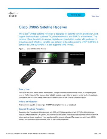
Transcription
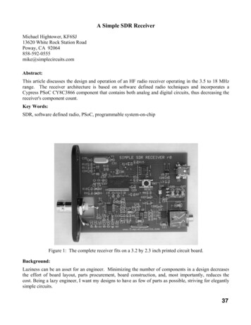
A Simple SDR ReceiverMichael Hightower, KF6SJ13620 White Rock Station RoadPoway, CA his article discusses the design and operation of an HF radio receiver operating in the 3.5 to 18 MHzrange. The receiver architecture is based on software defined radio techniques and incorporates aCypress PSoC CY8C3866 component that contains both analog and digital circuits, thus decreasing thereceiver's component count.Key Words:SDR, software defined radio, PSoC, programmable system-on-chipFigure 1: The complete receiver fits on a 3.2 by 2.3 inch printed circuit board.Background:Laziness can be an asset for an engineer. Minimizing the number of components in a design decreasesthe effort of board layout, parts procurement, board construction, and, most importantly, reduces thecost. Being a lazy engineer, I want my designs to have as few of parts as possible, striving for elegantlysimple circuits.37
During the last few years, I have built a few homebrew receivers using software defined radio (SDR)techniques. Each successive design is simpler, performs better, is less expensive, and uses fewcomponents than its predecessor. One of my favorite components to use is the Cypress SemiconductorPSoC series of components. These parts are far more than just a microcomputer; they also containsoftware configurable analog and digital peripherals on a single chip. Cypress calls the family a PSoCin reference to it being a programmable embedded system-on-chip. The newest series of parts, whichCypress calls the PSoC 3 family, contains a 67 MHz 8051 class microcomputer, an analog to digitalconverter fast enough and with enough resolution for an SDR receiver, and other valuable functions thatare desirable in a receiver design. When I saw this part, I immediately saw its use in an HF receiver.Receiver design goals:My goal was to use the PSoC 3 component as the cornerstone of an SDR receiver design. The receivershould be used for casual, conversational listening, not a higher performance receiver for DX use. Itshould also be built with a minimum number of components, small, and easy to use. I consideredadding an LCD display and controls to select the frequency and modes of operations, but decided thatthe design would have fewer parts and cost less if a PC is used for user input and output. Since thePSoC has a USB port, the receiver can connect to the PC with a USB cable and take power from the PCover the USB cable, saving a power jack, and external power source. Control of the receiver isaccomplished by the receiver USB port appearing as a standard com port to the PC. The Ham RadioDeluxe (HRD) program works perfectly to control this receiver.The basic SDR receiver:A common SDR receiver is built using a quadrature sampling detector, as shown in the block diagram offigure 2. The quadrature sampling detector is nothing more than a set of analog switches that areenabled and disabled in the particular sequence that samples the input signal four times for each cycle ofthe desired receive frequency. The four samples represent the 0, 90, 180, and 270 degrees of a sinewave. The output of the detector is amplified by a pair of op amp low-pass filters. After the op amps,the remaining signal processing is performed inside the PSoC microcomputer using digital processingtechniques. The processing will digitize the baseband signal, remove the undesired sideband from thereceived signal, limit the bandwidth of the audio, and then convert the digital samples back into ananalog audio signal.38
Low NoiseOpamp5KHz Low Pass25 MHzAntenna InputAnalogMuxLow Pass FilterLow NoiseOpamp5KHz Low PassClock GeneratorIQ90 Phase ShiftLogic8 MHz Reference39.26 KSPSADCDelay32 Tap19.63 KSPSDeMuxHilbertTransform64 Tap FIR or - for USB or LSBLow Pass Filter64 Tap FIR8 bit DACAudio OutputFigure 2: SDR Receiver block diagram.Circuit Description:At the antenna input terminals, an RF low pass filter having a 25 MHz corner frequency suppressessignals above the receiver tuning capability. Figure 3 shows the frequency response for the filter.39
Figure 3: Input RF Filter Response.Referring to the schematic in figures 6 and 7, U1, a dual 1-of-4 multiplexer/demultiplexer, is used as thesampling detector. This process is similar in functionality as a local mixer, only the control is performedwith digital logic switching levels.A Cirrus Logic clock generator chip, U7, is used to generate a microcomputer controller frequency. It iscalled a fractional-N clock multiplier and is basically a phase lock loop. The advantages of thiscomponent over a discrete digital synthesizer chip (DDS) is that is it cheaper, it has less phase jitter in itsoutput, and it outputs a logic level signal that can be connected directly to the sampling detectormultiplexer's control inputs without the need to add a comparator circuit to slice the DDS sine waveoutput. The clock generator operates at twice the desired receive frequency. The PSoC inputs this clocksignal, one rising edge divide by two circuit generates the I clock signal, another falling edge divide-bytwo circuit creates the Q clock signal. These two signals are output to the sampling detectormultiplexer. They are square waves at the desired receive frequency that are shifted by 90 from oneanother.Per the PSoC specification, its inputs are guaranteed to 33 MHz. That means that the clock generatorinput is the limiting factor in the upper frequency operating range of the receiver. Since this frequencyis twice the receive frequency, the highest guaranteed operation is 16.5 MHz. However, after testingseveral receivers, all have worked to at least 18 MHz (36 MHz clock input) which is near the 17 meteramateur band.After the mixing process, a pair low noise op amps, U2A and U2B, amplify the base band signals. Thepart was chosen because of its low noise performance and the ability to operate with inputs and outputsnear the ground and power rails. The inputs to the op amps are typically in the microvolt range. Sincethe op amp circuit voltage gain is on the order of 40 dB at 1 kHz, the output signals are on the order of afew hundred microvolts to a few millivolts. This circuit includes a first order low-pass filter having a 3kHz corner frequency. It is important to reduce the frequencies above half of the analog to digitalconverter sampling rate which is called the Nyquist frequency. Otherwise, images will appear atfrequencies near the sampling rate. Figure 4 shows the frequency response of the op amp circuit.40
Figure 4: Op amp circuit frequency response.From this point, all of the signal processing is performed in the digital domain, and, specifically, insidethe PSoC, U6.The PSoC has a single analog to digital converter (ADC). Since there are two base band signals toprocess, the I and the Q channels, an analog multiplexer is used to switch one of the two inputs to theADC input. It is desirable to have a high sample rate and a high number of bits, but the best tradeoff Icould find is to use the ADC in a 14 bit mode and sampling at 39,260 samples per second. Since asample from each input channel is necessary, the equivalent sample rate per channel is 19,630 samplesper second. Therefore, the Nyquist frequency is almost 10 kHz. The op amp frequency response at 10kHz is about 15 dB below the desired passband. This is not great, but leaves room for improvement in afuture version.The rest is all digital processing. The PSoC 3 family of parts have an interesting internal hardwarefeature they call a digital filter block, or DFB, and it consists of a 24-bit fixed point, programmablelimited scope DSP engine. This is a dedicated hardware accelerator block that operates independentlyof the main 8051 processor. It consists of a dedicated multiplier and accumulator that calculates a 24-bitby 24-bit multiply 48-bit accumulates in one system clock cycle. It is optimized to implement a directform Finite Impulse Response (FIR) filter that approaches a computation rate of one FIR tap for eachclock cycle. This block is used as two independent, 64 tap, digital filters.Alternating outputs from the ADC are loaded into either a 32 sample long delay line or one of the twodigital filters. This digital filter uses a set of coefficients that form an all-pass filter having a flatmagnitude response, but phase shifts all frequency in its passband by 90 . This is called a Hilbert filter.Suppressing either the upper or lower sideband is accomplished by phase shifting the Q channelbaseband data and either subtracting or adding the filter output to the delayed I channel baseband data.The delay is necessary to compensate only for the delays incurred by the processing of the Hilbert filter.The output of the addition is one of the two sidebands.After the removal of the undesired sideband, the data stream is feed into the other half of the PSoCdigital filter block configured as a low-pass filter. This filter has a steep rolloff as shown in the figure 5for a 2 kHz filter. This is the advantage of processing in the digital domain as compared to a set ofanalog filters. Steep rolloffs and repeatability of the filter performance over wide temperature rangesand from part to part variations are the reasons to use digital processing.The output of the low-pass filter is fed into one of the PSoC’s 8 bit digital to analog converters (DAC)that converts the data stream back into an analog signal. This signal is buffered with a unity gain opamp, U3, and passed to the output connector.41
Figure 5: PSoC Digital low-pass filter response.Operation:The PSoC has an internal USB full speed port. I wrote firmware for this device to implement a serialcommunication port. When connected to a personal computer, the receiver will look like a serial device.Using the standard CDC (communication) drivers that are built into Windows, the receiver cancommunicate with Ham Radio Deluxe. The receiver firmware uses the Elecraft K2 communicationprotocol. I chose this protocol because it was one of the few that I could find that had a writtenspecification available.The receiver's audio output will directly drive low impedance headsets. The use of good computerspeakers that have a built-in amplifier and volume adjustment is ideal. There is no volume controlcapability in the receiver. Headsets need their own volume adjustments.The radio works on all frequencies from 3.5 MHz to at least 18 MHz (80 to 17 meters).Any one of 4 different receive filter bandwidths can be selected using HRD. FL1 is a 2.5 KHz low passfilter, FL2 is a 2.0 KHz low pass filter, FL3 is a 1.5 KHz low pass filter, and FL4 is used for CW andRTTY and is a 1.0 KHz band pass filter that is 400 Hz wide ( /- 200 Hz).The attenuator button (ATT) will turn decrease the volume by several dB.Performance:The minimum discernible signal (MDS) is approximately -117 dBm. A typical receiver would normallybe more towards the -120 dBm number. However, on the lower HF frequencies, where atmospheric andman-made noise dominates, the performance is sufficient. In fact, in a head to head comparison with myFlex Radio Flex-3000, I find it difficult to hear any difference. Not bad for a 50 receiver.42
Figure 6: SDR Receiver schematic, sheet 1, digital.43
Figure 7: SDR Receiver schematic, sheet 2, RF.44
The receiver architecture is based on software defined radio techniques and incorporates a Cypress PSoC CY8C3866 component that contains both analog and digital circuits, thus decreasing the receiver's component count. Key Words: SDR, software