Transcription
Distributed by:www.Jameco.com 1-800-831-4242The content and copyrights of the attachedmaterial are the property of its owner.Jameco Part Number 1721643
Section I. Cyclone IIDevice Family Data SheetThis section provides information for board layout designers tosuccessfully layout their boards for Cyclone II devices. It contains therequired PCB layout guidelines, device pin tables, and packagespecifications.This section includes the following chapters:Revision HistoryAltera Corporation Chapter 1. Introduction Chapter 2. Cyclone II Architecture Chapter 3. Configuration & Testing Chapter 4. Hot Socketing & Power-On Reset Chapter 5. DC Characteristics and Timing Specifications Chapter 6. Reference & Ordering InformationRefer to each chapter for its own specific revision history. For informationon when each chapter was updated, refer to the Chapter Revision Datessection, which appears in the complete handbook.Section I–1Preliminary
Revision HistorySection I–2PreliminaryCyclone II Device Handbook, Volume 1Altera Corporation
1. IntroductionCII51001-3.2IntroductionFollowing the immensely successful first-generation Cyclone devicefamily, Altera Cyclone II FPGAs extend the low-cost FPGA densityrange to 68,416 logic elements (LEs) and provide up to 622 usable I/Opins and up to 1.1 Mbits of embedded memory. Cyclone II FPGAs aremanufactured on 300-mm wafers using TSMC's 90-nm low-k dielectricprocess to ensure rapid availability and low cost. By minimizing siliconarea, Cyclone II devices can support complex digital systems on a singlechip at a cost that rivals that of ASICs. Unlike other FPGA vendors whocompromise power consumption and performance for low-cost, Altera’slatest generation of low-cost FPGAs—Cyclone II FPGAs, offer 60% higherperformance and half the power consumption of competing 90-nmFPGAs. The low cost and optimized feature set of Cyclone II FPGAs makethem ideal solutions for a wide array of automotive, consumer,communications, video processing, test and measurement, and otherend-market solutions. Reference designs, system diagrams, and IP, foundat www.altera.com, are available to help you rapidly develop completeend-market solutions using Cyclone II FPGAs.Low-Cost Embedded Processing SolutionsCyclone II devices support the Nios II embedded processor which allowsyou to implement custom-fit embedded processing solutions. Cyclone IIdevices can also expand the peripheral set, memory, I/O, or performanceof embedded processors. Single or multiple Nios II embedded processorscan be designed into a Cyclone II device to provide additionalco-processing power or even replace existing embedded processors inyour system. Using Cyclone II and Nios II together allow for low-cost,high-performance embedded processing solutions, which allow you toextend your product's life cycle and improve time to market overstandard product solutions.Low-Cost DSP SolutionsUse Cyclone II FPGAs alone or as DSP co-processors to improveprice-to-performance ratios for digital signal processing (DSP)applications. You can implement high-performance yet low-cost DSPsystems with the following Cyclone II features and design support: Altera CorporationFebruary 2008Up to 150 18 18 multipliersUp to 1.1 Mbit of on-chip embedded memoryHigh-speed interfaces to external memory1–1
Features DSP intellectual property (IP) coresDSP Builder interface to The Mathworks Simulink and Matlabdesign environmentDSP Development Kit, Cyclone II EditionCyclone II devices include a powerful FPGA feature set optimized forlow-cost applications including a wide range of density, memory,embedded multiplier, and packaging options. Cyclone II devices supporta wide range of common external memory interfaces and I/O protocolsrequired in low-cost applications. Parameterizable IP cores from Alteraand partners make using Cyclone II interfaces and protocols fast and easy.FeaturesThe Cyclone II device family offers the following features: High-density architecture with 4,608 to 68,416 LEs M4K embedded memory blocks Up to 1.1 Mbits of RAM available without reducing availablelogic 4,096 memory bits per block (4,608 bits per block including 512parity bits) Variable port configurations of 1, 2, 4, 8, 9, 16, 18, 32,and 36 True dual-port (one read and one write, two reads, or twowrites) operation for 1, 2, 4, 8, 9, 16, and 18 modes Byte enables for data input masking during writes Up to 260-MHz operation Embedded multipliers Up to 150 18- 18-bit multipliers are each configurable as twoindependent 9- 9-bit multipliers with up to 250-MHzperformance Optional input and output registers Advanced I/O support High-speed differential I/O standard support, including LVDS,RSDS, mini-LVDS, LVPECL, differential HSTL, and differentialSSTL Single-ended I/O standard support, including 2.5-V and 1.8-V,SSTL class I and II, 1.8-V and 1.5-V HSTL class I and II, 3.3-V PCIand PCI-X 1.0, 3.3-, 2.5-, 1.8-, and 1.5-V LVCMOS, and 3.3-, 2.5-,and 1.8-V LVTTL Peripheral Component Interconnect Special Interest Group (PCISIG) PCI Local Bus Specification, Revision 3.0 compliance for 3.3-Voperation at 33 or 66 MHz for 32- or 64-bit interfaces PCI Express with an external TI PHY and an Altera PCI Express 1 Megacore function1–2Cyclone II Device Handbook, Volume 1Altera CorporationFebruary 2008
Introduction Altera CorporationFebruary 2008133-MHz PCI-X 1.0 specification compatibilityHigh-speed external memory support, including DDR, DDR2,and SDR SDRAM, and QDRII SRAM supported by drop inAltera IP MegaCore functions for ease of useThree dedicated registers per I/O element (IOE): one inputregister, one output register, and one output-enable registerProgrammable bus-hold featureProgrammable output drive strength featureProgrammable delays from the pin to the IOE or logic arrayI/O bank grouping for unique VCCIO and/or VREF banksettingsMultiVolt I/O standard support for 1.5-, 1.8-, 2.5-, and3.3-interfacesHot-socketing operation supportTri-state with weak pull-up on I/O pins before and duringconfigurationProgrammable open-drain outputsSeries on-chip termination support Flexible clock management circuitry Hierarchical clock network for up to 402.5-MHz performance Up to four PLLs per device provide clock multiplication anddivision, phase shifting, programmable duty cycle, and externalclock outputs, allowing system-level clock management andskew control Up to 16 global clock lines in the global clock network that drivethroughout the entire device Device configuration Fast serial configuration allows configuration times less than100 ms Decompression feature allows for smaller programming filestorage and faster configuration times Supports multiple configuration modes: active serial, passiveserial, and JTAG-based configuration Supports configuration through low-cost serial configurationdevices Device configuration supports multiple voltages (either 3.3, 2.5,or 1.8 V) Intellectual property Altera megafunction and Altera MegaCore function support,and Altera Megafunctions Partners Program (AMPPSM)megafunction support, for a wide range of embeddedprocessors, on-chip and off-chip interfaces, peripheralfunctions, DSP functions, and communications functions and1–3Cyclone II Device Handbook, Volume 1
Features protocols. Visit the Altera IPMegaStore at www.altera.com todownload IP MegaCore functions.Nios II Embedded Processor supportThe Cyclone II family offers devices with the Fast-On feature, whichoffers a faster power-on-reset (POR) time. Devices that support theFast-On feature are designated with an “A” in the device ordering code.For example, EP2C5A, EP2C8A, EP2C15A, and EP2C20A. The EP2C5A isonly available in the automotive speed grade. The EP2C8A and EP2C20Aare only available in the industrial speed grade. The EP2C15A is onlyavailable with the Fast-On feature and is available in both commercialand industrial grades. The Cyclone II “A” devices are identical in featureset and functionality to the non-A devices except for support of the fasterPOR time.fCyclone II A devices are offered in automotive speed grade. For moreinformation, refer to the Cyclone II section in the Automotive-Grade DeviceHandbook.fFor more information on POR time specifications for Cyclone II A andnon-A devices, refer to the Hot Socketing & Power-On Reset chapter in theCyclone II Device Handbook.Table 1–1 lists the Cyclone II device family features. Table 1–2 lists theCyclone II device package offerings and maximum user I/O pins.Table 1–1. Cyclone II FPGA Family Features (Part 1 of 2)FeatureEP2C5 (2)EP2C8 (2)EP2C15 (1)EP2C20 39,616483,840594,4321,152,000Embeddedmultipliers (3)131826263586150PLLs2244444LEsM4K RAM blocks (4Kbits plus512 parity bitsTotal RAM bits1–4Cyclone II Device Handbook, Volume 1Altera CorporationFebruary 2008
IntroductionTable 1–1. Cyclone II FPGA Family Features (Part 2 of 2)FeatureMaximum userI/O pinsEP2C5 (2)EP2C8 (2)EP2C15 (1)EP2C20 (2)EP2C35EP2C50EP2C70158182315315475450622Notes to Table 1–1:(1)(2)(3)The EP2C15A is only available with the Fast On feature, which offers a faster POR time. This device is available inboth commercial and industrial grade.The EP2C5, EP2C8, and EP2C20 optionally support the Fast On feature, which is designated with an “A” in thedevice ordering code. The EP2C5A is only available in the automotive speed grade. The EP2C8A and EP2C20Adevices are only available in industrial grade.This is the total number of 18 18 multipliers. For the total number of 9 9 multipliers per device, multiply thetotal number of 18 18 multipliers by 2.Altera CorporationFebruary 20081–5Cyclone II Device Handbook, Volume 1
FeaturesTable 1–2. Cyclone II Package Options & Maximum User I/O PinsDevice144-PinTQFP (3)208-Pin 240-PinPQFP (4) PQFP256-PinFineLineBGANotes (1) (2)484-PinFineLineBGA484-Pin672-Pin 896-PinUltraFineLine FineLineFineLineBGABGABGAEP2C5 (6) (8)89142—158 (5)————EP2C8 (6)85138—182————EP2C8A (6), (7)———182————EP2C15A (6), (7)———152315———EP2C20 (6)——142152315———EP2C20A (6), (7)———152315———EP2C35 (6)————322322475—EP2C50 (6)————294294450—EP2C70 (6)——————422622Notes to Table 1–2:(1)(2)(3)(4)(5)(6)(7)(8)Cyclone II devices support vertical migration within the same package (for example, you can migrate between theEP2C20 device in the 484-pin FineLine BGA package and the EP2C35 and EP2C50 devices in the same package).The Quartus II software I/O pin counts include four additional pins, TDI, TDO, TMS, and TCK, which are notavailable as general purpose I/O pins.TQFP: thin quad flat pack.PQFP: plastic quad flat pack.Vertical migration is supported between the EP2C5F256 and the EP2C8F256 devices. However, not all of the DQand DQS groups are supported. Vertical migration between the EP2C5 and the EP2C15 in the F256 package is notsupported.The I/O pin counts for the EP2C5, EP2C8, and EP2C15A devices include 8 dedicated clock pins that can be usedfor data inputs. The I/O counts for the EP2C20, EP2C35, EP2C50, and EP2C70 devices include 16 dedicated clockpins that can be used for data inputs.EP2C8A, EP2C15A, and EP2C20A have a Fast On feature that has a faster POR time. The EP2C15A is only availablewith the Fast On option.The EP2C5 optionally support the Fast On feature, which is designated with an “A” in the device ordering code.The EP2C5A is only available in the automotive speed grade. Refer to the Cyclone II section in the Automotive-GradeDevice Handbook.Cyclone II devices support vertical migration within the same package(for example, you can migrate between the EP2C35, EPC50, and EP2C70devices in the 672-pin FineLine BGA package). The exception to verticalmigration support within the Cyclone II family is noted in Table 1–3.1–6Cyclone II Device Handbook, Volume 1Altera CorporationFebruary 2008
IntroductionVertical migration means that you can migrate to devices whosededicated pins, configuration pins, and power pins are the same for agiven package across device densities.Table 1–3. Total Number of Non-Migratable I/O Pins for Cyclone II Vertical Migration PathsVertical144-Pin TQFPMigration Path208-PinPQFP256-Pin484-Pin672-Pin484-Pin UltraFineLine BGA FineLine BGAFineLine BGAFineLine BGA(1)(2)(3)EP2C5 toEP2C8441 (4)———EP2C8 toEP2C15——30———EP2C15 toEP2C20——00————16——EP2C20 toEP2C35EP2C35 toEP2C50———2828 (5)28EP2C50 toEP2C70————2828Notes to Table 1–3:(1)(2)(3)(4)(5)Vertical migration between the EP2C5F256 to the EP2C15AF256 and the EP2C5F256 to the EP2C20F256 devices isnot supported.When migrating from the EP2C20F484 device to the EP2C50F484 device, a total of 39 I/O pins are non-migratable.When migrating from the EP2C35F672 device to the EP2C70F672 device, a total of 56 I/O pins are non-migratable.In addition to the one non-migratable I/O pin, there are 34 DQ pins that are non-migratable.The pinouts of 484 FBGA and 484 UBGA are the same.1When moving from one density to a larger density, I/O pins areoften lost because of the greater number of power and groundpins required to support the additional logic within the largerdevice. For I/O pin migration across densities, you must crossreference the available I/O pins using the device pin-outs for allplanned densities of a given package type to identify which I/Opins are migratable.To ensure that your board layout supports migratable densities withinone package offering, enable the applicable vertical migration pathwithin the Quartus II software (go to Assignments menu, then Device,then click the Migration Devices button). After compilation, check theinformation messages for a full list of I/O, DQ, LVDS, and other pins thatare not available because of the selected migration path. Table 1–3 lists theCyclone II device package offerings and shows the total number ofnon-migratable I/O pins when migrating from one density device to alarger density device.Altera CorporationFebruary 20081–7Cyclone II Device Handbook, Volume 1
FeaturesCyclone II devices are available in up to three speed grades: –6, –7, and–8, with –6 being the fastest. Table 1–4 shows the Cyclone II devicespeed-grade offerings.Table 1–4. Cyclone II Device Speed 2-PinFineLineBGA896-PinFineLineBGAEP2C5 (1)–6, –7, –8–7, –8—–6, –7, –8————EP2C8–6, –7, –8–7, –8—–6, –7, C8A (2)EP2C15A———–6, –7, –8 –6, –7, –8———EP2C20——–8–6, –7, –8 –6, –7, –8———EP2C20A (2)———–8———EP2C35————–6, –7, –8 –6, –7, –8 –6, –7, –8—EP2C50————–6, –7, –8 –6, –7, –8 –6, –7, –8—EP2C70————–8——–6, –7, –8 –6, –7, –8Notes to Table 1–4:(1)(2)The EP2C5 optionally support the Fast On feature, which is designated with an “A” in the device ordering code.The EP2C5A is only available in the automotive speed grade. Refer to the Cyclone II section in the Automotive-GradeDevice Handbook for detailed information.EP2C8A and EP2C20A are only available in industrial grade.1–8Cyclone II Device Handbook, Volume 1Altera CorporationFebruary 2008
IntroductionReferencedDocumentsThis chapter references the following documents:DocumentRevision HistoryTable 1–5 shows the revision history for this document. Hot Socketing & Power-On Reset chapter in Cyclone II Device HandbookAutomotive-Grade Device HandbookTable 1–5. Document Revision HistoryDate &DocumentVersionFebruary 2008v3.2 February 2007v3.1 November 2005v2.1 July 2005 v2.0 Changes MadeSummary of ChangesAdded “Referenced Documents”.Updated “Features” section and Table 1–1, Table 1–2,and Table 1–4 with information about EP2C5A.—Added document revision history.Added new Note (2) to Table 1–2.Note to explain differencebetween I/O pin countinformation provided inTable 1–2 and in the Quartus IIsoftware documentation.Updated Introduction and Features.Updated Table 1–3.—Updated technical content throughout.Updated Table 1–2.Added Tables 1–3 and 1–4.—Updated Table 1–2.Updated bullet list in the “Features” section.—November 2004v1.1 June 2004 v1.0Added document to the Cyclone II Device Handbook. Altera CorporationFebruary 2008—1–9Cyclone II Device Handbook, Volume 1
Document Revision History1–10Cyclone II Device Handbook, Volume 1Altera CorporationFebruary 2008
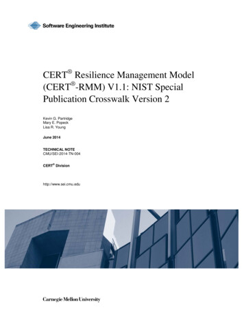
2. Cyclone II ne II devices contain a two-dimensional row- and column-basedarchitecture to implement custom logic. Column and row interconnectsof varying speeds provide signal interconnects between logic arrayblocks (LABs), embedded memory blocks, and embedded multipliers.The logic array consists of LABs, with 16 logic elements (LEs) in eachLAB. An LE is a small unit of logic providing efficient implementation ofuser logic functions. LABs are grouped into rows and columns across thedevice. Cyclone II devices range in density from 4,608 to 68,416 LEs.Cyclone II devices provide a global clock network and up to fourphase-locked loops (PLLs). The global clock network consists of up to 16global clock lines that drive throughout the entire device. The global clocknetwork can provide clocks for all resources within the device, such asinput/output elements (IOEs), LEs, embedded multipliers, andembedded memory blocks. The global clock lines can also be used forother high fan-out signals. Cyclone II PLLs provide general-purposeclocking with clock synthesis and phase shifting as well as externaloutputs for high-speed differential I/O support.M4K memory blocks are true dual-port memory blocks with 4K bits ofmemory plus parity (4,608 bits). These blocks provide dedicated truedual-port, simple dual-port, or single-port memory up to 36-bits wide atup to 260 MHz. These blocks are arranged in columns across the devicein between certain LABs. Cyclone II devices offer between 119 to1,152 Kbits of embedded memory.Each embedded multiplier block can implement up to either two 9 9-bitmultipliers, or one 18 18-bit multiplier with up to 250-MHzperformance. Embedded multipliers are arranged in columns across thedevice.Each Cyclone II device I/O pin is fed by an IOE located at the ends of LABrows and columns around the periphery of the device. I/O pins supportvarious single-ended and differential I/O standards, such as the 66- and33-MHz, 64- and 32-bit PCI standard, PCI-X, and the LVDS I/O standardat a maximum data rate of 805 megabits per second (Mbps) for inputs and640 Mbps for outputs. Each IOE contains a bidirectional I/O buffer andthree registers for registering input, output, and output-enable signals.Dual-purpose DQS, DQ, and DM pins along with delay chains (used toAltera CorporationFebruary 20072–1
Logic Elementsphase-align double data rate (DDR) signals) provide interface support forexternal memory devices such as DDR, DDR2, and single data rate (SDR)SDRAM, and QDRII SRAM devices at up to 167 MHz.Figure 2–1 shows a diagram of the Cyclone II EP2C20 device.Figure 2–1. Cyclone II EP2C20 Device Block LogicArrayLogicArrayLogicArrayIOEsM4K BlocksM4K BlocksPLLIOEsPLLThe number of M4K memory blocks, embedded multiplier blocks, PLLs,rows, and columns vary per device.Logic ElementsThe smallest unit of logic in the Cyclone II architecture, the LE, is compactand provides advanced features with efficient logic utilization. Each LEfeatures: A four-input look-up table (LUT), which is a function generator thatcan implement any function of four variablesA programmable registerA carry chain connectionA register chain connectionThe ability to drive all types of interconnects: local, row, column,register chain, and direct link interconnectsSupport for register packingSupport for register feedback2–2Cyclone II Device Handbook, Volume 1Altera CorporationFebruary 2007
Cyclone II ArchitectureFigure 2–2 shows a Cyclone II LE.Figure 2–2. Cyclone II LERegister ChainRouting FromPrevious LELAB-WideRegister ster SelectClearLAB SynchronousLoad andClear LogicDQProgrammableRegisterRow, Column,And Direct t(DEV CLRn)AsynchronousClear LogicRow, Column,And Direct LinkRoutingLocal RoutingClock &Clock EnableSelectRegisterFeedbackRegister ChainOutputlabclk1labclk2labclkena1labclkena2LAB Carry-OutEach LE’s programmable register can be configured for D, T, JK, or SRoperation. Each register has data, clock, clock enable, and clear inputs.Signals that use the global clock network, general-purpose I/O pins, orany internal logic can drive the register’s clock and clear control signals.Either general-purpose I/O pins or internal logic can drive the clockenable. For combinational functions, the LUT output bypasses theregister and drives directly to the LE outputs.Each LE has three outputs that drive the local, row, and column routingresources. The LUT or register output can drive these three outputsindependently. Two LE outputs drive column or row and direct linkrouting connections and one drives local interconnect resources, allowingthe LUT to drive one output while the register drives another output. Thisfeature, register packing, improves device utilization because the devicecan use the register and the LUT for unrelated functions. When usingregister packing, the LAB-wide synchronous load control signal is notavailable. See “LAB Control Signals” on page 2–8 for more information.Altera CorporationFebruary 20072–3Cyclone II Device Handbook, Volume 1
Logic ElementsAnother special packing mode allows the register output to feed back intothe LUT of the same LE so that the register is packed with its own fan-outLUT, providing another mechanism for improved fitting. The LE can alsodrive out registered and unregistered versions of the LUT output.In addition to the three general routing outputs, the LEs within an LABhave register chain outputs. Register chain outputs allow registers withinthe same LAB to cascade together. The register chain output allows anLAB to use LUTs for a single combinational function and the registers tobe used for an unrelated shift register implementation. These resourcesspeed up connections between LABs while saving local interconnectresources. See “MultiTrack Interconnect” on page 2–10 for moreinformation on register chain connections.LE Operating ModesThe Cyclone II LE operates in one of the following modes: Normal modeArithmetic modeEach mode uses LE resources differently. In each mode, six availableinputs to the LE—the four data inputs from the LAB local interconnect,the LAB carry-in from the previous carry-chain LAB, and the registerchain connection—are directed to different destinations to implement thedesired logic function. LAB-wide signals provide clock, asynchronousclear, synchronous clear, synchronous load, and clock enable control forthe register. These LAB-wide signals are available in all LE modes.The Quartus II software, in conjunction with parameterized functionssuch as library of parameterized modules (LPM) functions, automaticallychooses the appropriate mode for common functions such as counters,adders, subtractors, and arithmetic functions. If required, you can alsocreate special-purpose functions that specify which LE operating mode touse for optimal performance.Normal ModeThe normal mode is suitable for general logic applications andcombinational functions. In normal mode, four data inputs from the LABlocal interconnect are inputs to a four-input LUT (see Figure 2–3). TheQuartus II Compiler automatically selects the carry-in or the data3signal as one of the inputs to the LUT. LEs in normal mode supportpacked registers and register feedback.2–4Cyclone II Device Handbook, Volume 1Altera CorporationFebruary 2007
Cyclone II ArchitectureFigure 2–3. LE in Normal Modesloadsclear(LAB Wide) (LAB Wide)Packed Register InputRegister chainconnectionDRow, Column, andDirect Link RoutingENACLRNRow, Column, andDirect Link RoutingQdata1data2data3cin (from coutof previous LE)Four-InputLUTclock (LAB Wide)ena (LAB Wide)data4Local routingaclr (LAB Wide)Register FeedbackRegisterchain outputArithmetic ModeThe arithmetic mode is ideal for implementing adders, counters,accumulators, and comparators. An LE in arithmetic mode implements a2-bit full adder and basic carry chain (see Figure 2–4). LEs in arithmeticmode can drive out registered and unregistered versions of the LUToutput. Register feedback and register packing are supported when LEsare used in arithmetic mode.Altera CorporationFebruary 20072–5Cyclone II Device Handbook, Volume 1
Logic ElementsFigure 2–4. LE in Arithmetic Modesloadsclear(LAB Wide) (LAB Wide)Register chainconnectiondata1data2cin (from coutof previous LE)Three-InputLUTThree-InputLUTDRow, column, anddirect link routingENACLRNRow, column, anddirect link routingQclock (LAB Wide)ena (LAB Wide)Local routingaclr (LAB Wide)coutRegisterchain outputRegister FeedbackThe Quartus II Compiler automatically creates carry chain logic duringdesign processing, or you can create it manually during design entry.Parameterized functions such as LPM functions automatically takeadvantage of carry chains for the appropriate functions.The Quartus II Compiler creates carry chains longer than 16 LEs byautomatically linking LABs in the same column. For enhanced fitting, along carry chain runs vertically, which allows fast horizontal connectionsto M4K memory blocks or embedded multipliers through direct linkinterconnects. For example, if a design has a long carry chain in a LABcolumn next to a column of M4K memory blocks, any LE output can feedan adjacent M4K memory block through the direct link interconnect.Whereas if the carry chains ran horizontally, any LAB not next to thecolumn of M4K memory blocks would use other row or columninterconnects to drive a M4K memory block. A carry chain continues asfar as a full column.2–6Cyclone II Device Handbook, Volume 1Altera CorporationFebruary 2007
Cyclone II ArchitectureLogic ArrayBlocksEach LAB consists of the following: 16 LEsLAB control signalsLE carry chainsRegister chainsLocal interconnectThe local interconnect transfers signals between LEs in the same LAB.Register chain connections transfer the output of one LE’s register to theadjacent LE’s register within an LAB. The Quartus II Compiler placesassociated logic within an LAB or adjacent LABs, allowing the use oflocal, and register chain connections for performance and area efficiency.Figure 2–5 shows the Cyclone II LAB.Figure 2–5. Cyclone II LAB StructureRow InterconnectColumnInterconnectDirect linkinterconnectfrom adjacentblockDirect linkinterconnectfrom adjacentblockDirect linkinterconnectto adjacentblockDirect linkinterconnectto adjacentblockLABAltera CorporationFebruary 2007Local Interconnect2–7Cyclone II Device Handbook, Volume 1
Logic Array BlocksLAB InterconnectsThe LAB local interconnect can drive LEs within the same LAB. The LABlocal interconnect is driven by column and row interconnects and LEoutputs within the same LAB. Neighboring LABs, PLLs, M4K RAMblocks, and embedded multipliers from the left and right can also drivean LAB’s local interconnect through the direct link connection. The directlink connection feature minimizes the use of row and columninterconnects, providing higher performance and flexibility. Each LE candrive 48 LEs through fast local and direct link interconnects. Figure 2–6shows the direct link connection.Figure 2–6. Direct Link ConnectionDirect link interconnect fromright LAB, M4K memoryblock, embedded multiplier,PLL, or IOE outputDirect link interconnect fromleft LAB, M4K memoryblock, embedded multiplier,PLL, or IOE outputDirect linkinterconnectto rightDirect linkinterconnectto leftLocalInterconnectLABLAB Control SignalsEach LAB contains dedicated logic for driving control signals to its LEs.The control signals include: Two clocksTwo clock enablesTwo asynchronous clearsOne synchronous clearOne synchronous load2–8Cyclone II Device Handbook, Volume 1Altera CorporationFebruary 2007
Cyclone II ArchitectureThis gives a maximum of seven control signals at a time. When using theLAB-wide synchronous load, the clkena of labclk1 is not available.Additionally, register packing and synchronous load cannot be usedsimultaneously.Each LAB can have up to four non-global control signals. Additional LABcontrol signals can be used as long as they are global signals.Synchronous clear and load signals are useful for implementing countersand other functions. The synchronous clear and synchronous load signalsare LAB-wide signals that affect all registers in the LAB.Each LAB can use two clocks and two clock enable signals. Each LAB’sclock and clock enable signals are linked. For example, any LE in aparticular LAB using the labclk1 signal also uses labclkena1. If theLAB uses both the rising and falling edges of a clock, it also uses bothLAB-wide clock signals. De-asserting the clock enable signal turns off theLAB-wide clock.The LAB row clocks [5.0] and LAB local interconnect generate the LABwide control signals. The MultiTrack interconnect’s inherent low skewallows clock and control signal distribution in addition to data. Figure 2–7shows the LAB control signal generation circuit.Figure 2–7. LAB-Wide Control SignalsDedicatedLAB bclk1labclk2synclrlabclr1syncloadlabclr2LAB-wide signals control the logic for the register’s clear signal. The LEdirectly supports an asynchronous clear function. Each LAB supports upto two asynchronous clear signals (labclr1 and labclr2).Altera CorporationFebruary 20072–9Cyclone II Device Handbook, Volume 1
MultiTrack InterconnectA LAB-wide asynchronous load signal to control the logic for theregister’s preset signal is not available. The register preset is achieved byusing a NOT gate push-back technique. Cyclone II devices can onlysupport either a preset or asynchronous clear signal.In addition
DSP Development Kit, Cyclone II Edition Cyclone II devices include a powerful FPGA feature set optimized for low-cost applications including a wide range of density, memory, embedded multiplier, and packaging op tions. Cyclone II devices support a wide range of common external memory interfaces and I/O protocols required in low-cost applications.