Transcription
C8051F500DKC8051F500 D EVELOPMENT K IT U S E R ’ S G UIDE1. Relevant DevicesThe C8051F500 Development Kit is intended as a development platform for the microcontrollers in the C8051F50xMCU family. The members of this MCU family are: C8051F500, C8051F501, C8051F502, C8051F503,C8051F504, C8051F505, C8051F506, and C8051F507.The target board included in this kit is provided with a pre-soldered C8051F500 MCU (QFP48 package) and aC8051F502 (QFN32 package).Code developed on the C8051F500 can be easily ported to the other members of this MCU family.Refer to the C8051F50x data sheet for the differences between the members of this MCU family.2. Kit ContentsThe C8051F500 Development Kit contains the following items:C8051F500 Target BoardC8051Fxxx Development Kit Quick-Start GuideSilicon Laboratories IDE and Product Information CD-ROM. CD content includes:Silicon Laboratories Integrated Development Environment (IDE)Keil 8051 Development Tools (macro assembler, linker, evaluation ‘C’ compiler)Source code examples and register definition filesDocumentationC8051F500 Development Kit User’s Guide (this document)AC to DC Power AdapterUSB Debug Adapter (USB to Debug Interface)Two USB Cables3. Getting StartedThe necessary software to download, debug, and communicate with the target microcontroller is included in theCD-ROM. The following software is necessary to build a project, download code to, and communicate with thetarget microcontroller:Silicon Laboratories Integrated Development Environment (IDE)Keil 8051 Development Tools (macro assembler, linker, evaluation ‘C’ compiler)Other useful software that is provided in the CD-ROM includes:Configuration Wizard 2Keil uVision DriversCP210x USB to UART Virtual COM Port (VCP) DriversRev. 0.1 6/08Copyright 2008 by Silicon LaboratoriesC8051F500DK
C8051F500DK3.1. Software InstallationThe included CD-ROM contains the Silicon Laboratories Integrated Development Environment (IDE), Keil software8051 tools and additional documentation. Insert the CD-ROM into your PC’s CD-ROM drive. An installer willautomatically launch, allowing you to install the IDE software or read documentation by clicking buttons on theInstallation Panel. If the installer does not automatically start when you insert the CD-ROM, run autorun.exe foundin the root directory of the CD-ROM. Refer to the ReleaseNotes.txt file on the CD-ROM for the latest informationregarding known problems and restrictions. After installing the software, see the following sections for informationregarding the software and running one of the demo applications.3.2. CP210x USB to UART VCP Driver InstallationThe C8051F500 Target Board includes a Silicon Laboratories CP2102 USB-to-UART Bridge Controller. Devicedrivers for the CP2102 need to be installed before PC software such as HyperTerminal can communicate with thetarget board over the USB connection. If the "Install CP210x Drivers" option is selected during installation, a driver“unpacker” utility will launch.1. Follow the steps to copy the driver files to the desired location. The default directory is C:\SiLabs\MCU\CP210x.2. The final window will give an option to install the driver on the target system. Select the “Launch the CP210x VCP DriverInstaller” option if you are ready to install the driver.3. If selected, the driver installer will now launch, providing an option to specify the driver installation location. After pressingthe “Install” button, the installer will search your system for copies of previously installed CP210x Virtual COM Port drivers. Itwill let you know when your system is up to date. The driver files included in this installation have been certified by Microsoft.4. If the “Launch the CP210x VCP Driver Installer” option was not selected in step 3, the installer can be found in the locationspecified in step 2, by default C:\SiLabs\MCU\CP210x\Windows 2K XP S2K3 Vista. At this location runCP210xVCPInstaller.exe.5. To complete the installation process, connect the included USB cable between the host computer and the USB connector(P5) on the C8051F500 Target Board. Windows will automatically finish the driver installation. Information windows will popup from the taskbar to show the installation progress.6. If needed, the driver files can be uninstalled by selecting “Silicon Laboratories CP210x USB to UART Bridge (DriverRemoval” option in the “Add or Remove Programs” window.4. Software Overview4.1. Silicon Laboratories IDEThe Silicon Laboratories IDE integrates a source-code editor, a source-level debugger, and an in-system Flashprogrammer. See Section 6. "Using the Keil Software 8051 Tools with the Silicon Laboratories IDE‚" on page 5 fordetailed information on how to use the IDE. The Keil Evaluation Toolset includes a compiler, linker, and assemblerand easily integrates into the IDE. The use of third-party compilers and assemblers is also supported.4.1.1. IDE System RequirementsThe Silicon Laboratories IDE requirements:Pentium-class host PC running Microsoft Windows 2000 or newer.One available USB port.64 MB RAM and 40 MB free HD space recommended.4.1.2. Third Party ToolsetsThe Silicon Laboratories IDE has native support for many 8051 compilers. The full list of natively supported tools is:KeilIARRaisonanceTaskingHi-TechSDCCPlease note that the demo applications for the C8051F500 target board are written to work with the Keil and SDCCtoolsets.2Rev. 0.1
C8051F500DK4.2. Keil Evaluation Toolset4.2.1. Keil Assembler and LinkerThe assembler and linker that are part of the Keil Demonstration Toolset are the same versions that are found inthe full Keil Toolset. The complete assembler and linker reference manual can be found on-line under the Helpmenu in the IDE or in the “SiLabs\MCU\hlp” directory (A51.pdf).4.2.2. Keil Evaluation C51 C CompilerThe evaluation version of the C51 compiler is the same as the full version with these limitations: (1) Maximum 4 kBcode generation, and (2) Floating point library not included. When installed from the CD-ROM, the C51 compiler isinitially limited to a code size of 2 kB, and programs start at code address 0x0800. Please refer to the ApplicationNote “AN104: Integrating Keil Tools into the Silicon Labs IDE" for instructions to change the limitation to 4 kB, andhave the programs start at code address 0x0000.4.3. Configuration Wizard 2The Configuration Wizard 2 is a code generation tool for all of the Silicon Laboratories devices. Code is generatedthrough the use of dialog boxes for each of the device's peripherals.Figure 1. Configuration Wizard 2 UtilityThe Configuration Wizard 2 utility helps accelerate development by automatically generating initialization sourcecode to configure and enable the on-chip resources needed by most design projects. In just a few steps, the wizardcreates complete startup code for a specific Silicon Laboratories MCU. The program is configurable to provide theoutput in C or assembly. For more information, please refer to the Configuration Wizard 2 help available under theHelp menu in Config Wizard 2.Rev. 0.13
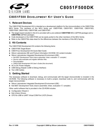
C8051F500DK4.4. Keil uVision2 and uVision3 Silicon Laboratories DriversAs an alternative to the Silicon Laboratories IDE, the uVision debug driver allows the Keil uVision IDE tocommunicate with Silicon Laboratories on-chip debug logic. In-system Flash memory programming integrated intothe driver allows for rapidly updating target code. The uVision IDE can be used to start and stop programexecution, set breakpoints, check variables, inspect and modify memory contents, and single-step throughprograms running on the actual target hardware.For more information, please refer to the uVision driver documentation. The documentation and software areavailable from the Downloads webpage (www.silabs.com/mcudownloads).5. Hardware Setup using a USB Debug AdapterThe target board is connected to a PC running the Silicon Laboratories IDE via the USB Debug Adapter as shownin Figure 2.1. Connect the USB Debug Adapter to one of the DEBUG connector on the target board (DEBUG A orDEBUG B) with the 10-pin ribbon cable. The recommended connection is to DEBUG A as this microcontroller is the primary MCU on the board and more peripherals are easily available.2. Connect one end of the USB cable to the USB connector on the USB Debug Adapter.3. Connect the other end of the USB cable to a USB Port on the PC.4. Connect the AC/DC power adapter to power jack P4 on the target board.Notes: Use the Reset button in the IDE to reset the target when connected using a USB Debug Adapter. Remove power from the target board and the USB Debug Adapter before connecting or disconnecting theribbon cable from the target board. Connecting or disconnecting the cable when the devices have power candamage the device and/or the USB Debug Adapter.PCP3J29RESET BDEBUG BP1.4 BP1.3 BDS1J11C8051F500-TBJ28Port 2 “B”Port 1 “B”J8J32U2F502J31J26SIDE “B”Port 0 “B”J27Target BoardGNDCAN LTB3PowerRunUSBCableStopP2Silicon LaboratoriesUSB DEBUG ADAPTERDEBUG AJ3J4Port 2 “A”P1.4 ARESET AJ18J19J7P4J21J9J10C8051F500P1.3 ADS2J5SIDE “A”Port 4 “A”Port 3 “A”J20R27P1U5COMMJ1 DS4Port 0 “A”J2 LIN VP1Port 1 “A”LIN OUTU1DS3J24J22www.silabs.comGNDJ14PWRJ17SILICON LABSCAN HAC/DCAdapterUSB DebugAdapterFigure 2. Hardware Setup using a USB Debug Adapter4Rev. 0.1
C8051F500DK6. Using the Keil Software 8051 Tools with the Silicon Laboratories IDETo perform source-level debugging with the IDE, you must configure the Keil 8051 tools to generate an absoluteobject file in the OMF-51 format with object extensions and debug records enabled. You may build the OMF-51absolute object file by calling the Keil 8051 tools at the command line (e.g., batch file or make file) or by using theproject manager built into the IDE. The default configuration when using the Silicon Laboratories IDE projectmanager enables object extension and debug record generation. Refer to Application Note "AN104: Integrating Keil8051 Tools into the Silicon Labs IDE" in the “SiLabs\MCU\Documentation\ApplicationNotes” directory for additionalinformation on using the Keil 8051 tools with the Silicon Laboratories IDE.To build an absolute object file using the Silicon Laboratories IDE project manager, you must first create a project.A project consists of a set of files, IDE configuration, debug views, and a target build configuration (list of files andtool configurations used as input to the assembler, compiler, and linker when building an output object file).The following sections illustrate the steps necessary to manually create a project with one or more source files,build a program, and download the program to the target in preparation for debugging. (The IDE will automaticallycreate a single-file project using the currently open and active source file if you select Build/Make Project before aproject is defined.)6.1. Creating a New Project1. Select Project New Project to open a new project and reset all configuration settings to default.2. Select File New File to open an editor window. Create your source file(s) and save the file(s) with arecognized extension, such as .c, .h, or .asm, to enable color syntax highlighting.3. Right-click on “New Project” in the Project Window. Select Add files to project. Select files in the filebrowser and click Open. Continue adding files until all project files have been added.4. For each of the files in the Project Window that you want assembled, compiled, and linked into the targetbuild, right-click on the file name and select Add file to build. Each file will be assembled or compiled asappropriate (based on file extension) and linked into the build of the absolute object file.Note: If a project contains a large number of files, the “Group” feature of the IDE can be used to organize thefiles. Right-click on “New Project” in the Project Window. Select Add Groups to project. Add pre-definedgroups or add customized groups. Right-click on the group name and choose Add file to group. Select filesto be added. Continue adding files until all project files have been added.Rev. 0.15
C8051F500DK6.2. Building and Downloading the Program for Debugging1. Once all source files have been added to the target build, build the project by clicking on the Build/MakeProject button in the toolbar or selecting Project Build/Make Project from the menu.Note: After the project has been built the first time, the Build/Make Project command will only build thefiles that have been changed since the previous build. To rebuild all files and project dependencies, clickon the Rebuild All button in the toolbar or select Project Rebuild All from the menu.2. Before connecting to the target device, several connection options may need to be set. Open theConnection Options window by selecting Options Connection Options. in the IDE menu. First, selectthe appropriate adapter in the “Serial Adapter” section. Next, the correct “Debug Interface” must be selected.C8051F50x family devices use the Silicon Labs 2-wire (C2) debug interface. Once all the selections are made,click the OK button to close the window.3. Click the Connect button in the toolbar or select Debug Connect from the menu to connect to the device.4. Download the project to the target by clicking the Download Code button in the toolbar.Note: To enable automatic downloading if the program build is successful, select Enable automaticconnect/download after build in the Project Target Build Configuration dialog. If errors occur duringthe build process, the IDE will not attempt the download.5. Save the project when finished with the debug session to preserve the current target build configuration,editor settings and the location of all open debug views. To save the project, select Project Save ProjectAs. from the menu. Create a new name for the project and click on Save.7. Example Source CodeExample source code and register definition files are provided in the “SiLabs\MCU\Examples\C8051F50x 1x\”directory during IDE installation. These files may be used as a template for code development. Exampleapplications include a blinking LED example which configures the green LED on the target board to blink at a fixedrate.7.1. Register Definition FilesRegister definition files C8051F500.inc and C8051F500 defs.h define all SFR registers and bit-addressablecontrol/status bits. A macro definition header file compiler defs.h is also included, and is required to be able to usethe C8051F500 defs.h header file with various tool chains. These files are installed into the“SiLabs\MCU\Examples\C8051F50x 1x\Header Files\” directory during IDE installation by default. The registerand bit names are identical to those used in the C8051F50x data sheet. These register definition files are alsoinstalled in the default search path used by the Keil Software 8051 tools. Therefore, when using the Keil 8051 toolsincluded with the development kit (A51, C51), it is not necessary to copy a register definition file to each project’sfile directory.7.2. Blinking LED ExampleThe example source files F500 Blinky.asm and F500 Blinky.c installed in the default directory“SiLabs\MCU\Examples\C8051F50x 1x\Blinky” show examples of several basic C8051F500 functions. Theseinclude disabling the watchdog timer (WDT), configuring the Port I/O crossbar, configuring a timer for an interruptroutine, initializing the system clock, and configuring a GPIO port pin. When compiled/assembled and linked, thisprogram flashes the green LED on the C8051F500 target board about five times a second using the interrupthandler with a C8051F500 timer.6Rev. 0.1
C8051F500DK8. Target BoardThe C8051F500 Development Kit includes a target board with a C8051F500 (Side A) and C8051F502 (Side B)device pre-installed for evaluation and preliminary software development. Numerous input/output (I/O) connectionsare provided to facilitate prototyping using the target board. Refer to Figure 3 for the locations of the various I/Oconnectors. Figure 4 on page 9 shows the factory default shorting block positions. A summary of the signal namesand headers is provided in Table 11 on page 16.J1-J5J7J8J9, J10J11J14J17J18Side A: Port 0 through Port 4 headersHeader to choose between 5V from Debug Adapter (P2) or 5V from on-board regulator (U6)Side B: CAN Transceiver (U4) power connectorSide A: External crystal enable connectorsSide B: Connects P1.3 B LED and P1.4 B Switch to MCU port pinsSide A: CAN Transceiver (U3) power connectorSide A: Connects MCU to three separate transceivers (UART(U5), CAN(U3) and LIN(T1))Side A: Connects VIO to VIO A SRC which powers the P1.2 potentiometer, the/RST A pin pull-up, and P1.4 A Switch pull-up.J19Side A: Connects P1.3 A LED and P1.4 A Switch to MCU port pinsJ20Side A: Connects R27 potentiometer to port pin 1.2J21Connect V HIGH node from TB1 LIN header to 5V regulator input for board powerJ22Side A: Connects decoupling capacitors C28 and C29 for MCU VREF (P0.0)J24Side A: Connects 5V net to VIO and VREGIN of the MCUJ26Side B: Connects MCU to three separate transceivers (CAN (U4) and LIN (T2))J27-J29 Side B: Port 0 through Port 2 headersJ31Side B: Connects 5V net to VIO and VREGIN of the MCUJ32Side B: Connects decoupling capacitors C41 and C42 for MCU VREF (P0.0)P1Side A: 96-pin female connectorP2Side A: DEBUG connector for Debug Adapter interfaceP3Side B: DEBUG connector for Debug Adapter interfaceP4Power connector (accepts input from 7 to 15 VDC unregulated power adapter)P5USB connector (connects to PC for serial communication)TB1Shared LIN Connector for Side A and B MCUs for external nodesTB2Shared CAN Connector for Side A and B MCUs for external nodesTB3Side A: Power supply terminal blockRev. 0.17
C8051F500DK12P1.4 A1J721J2P2GNDCAN L1P1.4 BJ21DS3PWRP1.3 BDS1DEBUG B1TB3P3Figure 3. C8051F500 Target Board with Pin Numbers8Rev. 0.112J28Port 2 “B”2C8051F500-TB1P42J27Port 1 “B”J11www.silabs.comJ32F5021SILICON LABSRESET ADEBUG AJ322J912J31J24 2J19Port 1 “A”U21U1J102J17J18Port 2 “A”Port 0 “B”1J22C8051F50021J41J261P1.3 ADS2Port 3 “A”22SIDE “A”J5SIDE “B”J8J14J20Port 4 “A”GNDCOMMDS4J1CAN H2R27U51TB2TB1P5 LIN VPort 0 “A”LIN OUTP11J29RESET B
C8051F500DK8.1. Target Board Shorting Blocks: Factory DefaultsThe C8051F500 target board comes from the factory with pre-installed shorting blocks on many headers. Figure 4shows the positions of the factory default shorting blocks.Port 0 “A”SIDE “B”GNDCAN LCAN HJ8J14J20Port 4 “A”GNDR27U5COMMJ1 DS4 LIN VP1LIN OUTP1J26Port 0 “B”SIDE “A”J5Port 3 “A”J22C8051F500P1.3 ADS2J17U2J18Port 2 “A”Port 2 “B”J9SILICON LABSP1.4 Bwww.silabs.comRESET AJ7Port 1 “A”J21DS3PWRP2P1.3 BDS1C8051F500-TBDEBUG AJ2J28J11J10J3Port 1 “B”F502J24J19J4J32U1P1.4 AJ27J31DEBUG BP4TB3J29RESET BP3Figure 4. C8051F500 Target Board Shorting Blocks: Factory DefaultsRev. 0.19
C8051F500DK8.2. Target Board Power Options and Current MeasurementThe C8051F500 target board supports three power options:1. 12V DC power using the AC to DC power adapter (P4)2. 5V DC USB VBUS power from PC via the USB Debug Adapter (DEBUG A)3. 12V DC power from the LIN external header (TB1)The two 12V power sources are ORed together using reverse-biased diodes (Z1 and Z2). The ORed power isregulated to a 5.0V DC voltage using a LDO regulator (U6). To power the board from the USB Debug Adapterconnected to DEBUG A instead of the 12V sources, move the shorting block on the J7 header to pins 2 and 3 toselect SER PWR. The output of the regulator powers the 5VD net on the target board, and is also connected toone end of the header J24 (SIDE A) and J31 (SIDE B). Two shorting blocks can be put on each header to connectthe 5V net to the VREGIN and VIO pins on the two MCUs. With the shorting block removed, a source meter can beused across the headers to measure the current consumption of the MCU.Note: The USB Debug Adapter does not provide the necessary peak power for the CAN transceivers to operate. One of the12V DC sources is recommended for CAN transceiver operation.8.3. System Clock Sources8.3.1. Internal OscillatorsThe C8051F500 and C8051F502 devices installed on the target board feature a factory calibrated programmablehigh-frequency internal oscillator (24 MHz base frequency, 0.5%), which is enabled as the system clock source onreset. After reset, the internal oscillator operates at a frequency of 187.5 kHz by default but may be configured bysoftware to operate at other frequencies. The on-chip crystal is accurate for CAN and LIN master communicationsand in many applications an external oscillator is not required. However, if you wish to operate the C8051F500device (SIDE A) at a frequency not available with the internal oscillator, an external crystal may be used. Refer tothe C8051F50x data sheet for more information on configuring the system clock source.8.3.2. External Oscillator OptionsThe target board is designed to facilitate the installation of an external crystal. Remove shorting blocks at headersJ9 and J10 and install the crystal at the pads marked Y1. Install a 10 MΩ resistor at R9 and install capacitors at C6and C7 using values appropriate for the crystal you select. If you wish to operate the external oscillator in capacitoror RC mode, options to install a capacitor or an RC network are also available on the target board. Populate C6 forcapacitor mode, and populate R3 and C6 for RC mode. Refer to the C8051F50x data sheet for more information onthe use of external oscillators.10Rev. 0.1
C8051F500DK8.4. Switches and LEDsTwo push-button switches are provided on the target board for each MCU. Switch RESET A is connected to the/RST pin of the C8051F500. Switch RESET B is connected to the /RST pin of the C8051F502. PressingRESET A puts the C8051F500 device into its hardware-reset state, and similarly for RESET B and theC8051F502 MCU. Switches P1.4 A and P1.4 B are connected to the MCU’s general purpose I/O (GPIO) pinsthrough headers. Pressing either one of these switches generates a logic low signal on the port pin. Remove theshorting block from the header to disconnect these switches from the port pins. See Table 1 for the port pins andheaders corresponding to each switch.Four LEDs are provided on the target board to serve as indicators. The red LED labeled PWR indicates presenceof power to the target board. The second red LED labeled COMM indicates if the CP2102 USB-to-UART bridge(P5) is recognized by the PC. The green LED labeled with port pin name P1.3 A is connected to the C8051F500’s(Side A) GPIO pin P1.3 through the header J19. Remove the shorting block from the header to disconnect the LEDfrom the port pin. Similarly, the green LED named P1.3 B is connected to the C8051F502 (Side B) through the J11header. See Table 1 for the port pins and headers corresponding to each LED.Table 1. Target Board I/O DescriptionsDescriptionI/OHeader(s)RESET ARESET BP1.4 A SwitchP1.4 B SwitchP1.3 A LEDP1.3 B LEDRed LED (PWR)Red LED (COMM)Reset (Side A)Reset (Side B)P1.4 (Side A)P1.4 (Side B)P1.3 (Side A)P1.3 (Side B)PowerCOMM �4]nonenone8.5. Target Board Debug Interfaces (P2 and P3)The debug connectors P2 (DEBUG A) and P3 (DEBUG B) provide access to the debug (C2) pins of theC8051F500 and C8051F502. The debug connectors are used to connect the Serial Adapter or the USB DebugAdapter to the target board for in-circuit debugging and Flash programming. Table 2 shows the DEBUG pindefinitions.Table 2. DEBUG Connector Pin DescriptionsPin #12, 3, 94567810Side A - C8051F500DescriptionPin #Not ConnectedGND (Ground)C2D A/RST (Reset)Not Connected/RST/C2CK ANot ConnectedUSB Power ( 5VDC from P2)12, 3, 94567810Rev. 0.1Side B - C8051F502DescriptionNot ConnectedGND (Ground)P3.0 C2D B/RST B (Reset)P3.0 B/RST/C2CK BNot ConnectedNot Connected11
C8051F500DK8.6. Serial Interface (P5)A USB-to-UART bridge circuit (U5) and USB connector (P5) are provided on the target board to facilitate serialconnections to UART0 of the C8051F500 (Side A). The Silicon Labs CP2102 USB-to-UART bridge provides dataconnectivity between the C8051F500 and the PC via a USB port. The TX and RX signals of UART0 may beconnected to the CP2102 by installing shorting blocks on header J17. The shorting block positions for connectingeach of these signals to the CP2102 are listed in Table 3. To use this interface, the USB-to-UART device driversshould be installed as described in Section 3.2. "CP210x USB to UART VCP Driver Installation‚" on page 2.Table 3. Serial Interface Header (J3) DescriptionHeader Pins UART0 Pin DescriptionJ17[9–10]J17[11–12]UART TX (P0.4 A)UART RX (P0.5 A)8.7. CAN Interface and Network (TB2)Both MCUs on the target board are connected to CAN transceivers through headers. The port pins assigned to theCAN peripheral on each MCU are P0.6 (CAN TX) and P0.7 (CAN RX). The C8051F500 (Side A) is connected toU3 through the J17 header and the C8051F502 (Side B) is connected to U4 through the J26 header. The two CANtransceivers are connected to each other and form a CAN network. Other external devices can be connected to theCAN network through the TB2 interface. The shorting block positions for connecting the MCUs to the CANtransceivers are listed in Table 4. The pin connections for the external CAN devices are listed in Table 5. The CANtransceivers are powered by the 5VREG node and connected through J8 and J14 headers.Table 4. CAN Interface Headers (J17 and J26) DescriptionHeader Pins CAN0 Pin ]CAN TX (P0.6 A)CAN RX (P0.7 A)CAN TX (P0.6 B)CAN RX (P0.7 B)Table 5. TB2 External CAN Interface Header Description12Pin #Pin Description123CAN HCAN LGNDRev. 0.1
C8051F500DK8.8. LIN Interface and Network (TB1)Both MCUs on the target board are connected to LIN transceivers through headers. These headers assume thatthe MCU’s crossbars are configured to put the LIN TX and RX pins on port pins P1.0 and P1.1 respectively. Seethe C8051F50x data sheet for crossbar configuration. The C8051F500 (Side A) is connected to the T1 transceiverthrough the J17 header and the C8051F502 (Side B) is connected to the T2 transceiver through the J26 header.The two LIN transceivers are connected to each other and form a LIN network. Other external devices can beconnected to the LIN network through the TB1 interface. The TB1 interface also provides the option for connectingan external power source so that all LIN transceivers can use the same source voltage. This source voltage canalso be used to power the target board. If an external voltage source is not provided, the LIN transceivers use the12V provided through the P4 wall-wart connector. See Section 8.2. for more power option details. The shortingblock positions for connecting the MCUs to the LIN transceivers are listed in Table 6. The pin connections for theexternal LIN devices are listed in Table 7.Table 6. LIN Interface Headers (J17 and J26) DescriptionHeader PinsLIN0 Pin LIN TX (P1.0 A)LIN RX (P1.1 A)LIN TX (P1.0 B)LIN RX (P1.1 B)Table 7. TB1 External LIN Interface Header DescriptionPin #Pin Description123 LIN VLIN OUTGND8.9. Port I/O Connectors (J1-J5 and J27-J29)Each of the parallel ports of the C8051F500 (Side A) and C8051F502 (Side B) has its own 10-pin headerconnector. Each connector provides a pin for the corresponding port pins 0-7, 5V VIO, and digital ground. Thesame pin-out is used for all of the port connectors.Table 8. Port I/O Connector Pin DescriptionPin #Pin Pn.7 5V (VIO)GND (Ground)Rev. 0.113
C8051F500DK8.10. Voltage Reference (VREF) Connectors (J22 and J32)The VREF connectors can be used to connect the VREF pin from the MCU (P0.0) to external 0.1 uF and 4.7 uFdecoupling capacitors. The C8051F500 (Side A) device is connected to the capacitors through the J22 header andthe C8051F502 (Side B) device connects to its own set of capacitors through J32.8.11. Expansion Connector (P1)The 96-pin expansion I/O connector P1 is used to connect daughter boards to the main target board. P1 providesaccess to many C8051F500 signal pins. Pins for VREGIN, VDD, VIO, and 3.3V are also available. See Table 9 fora complete list of pins available at P1.The P1 socket connector is manufactured by Hirose Electronic Co. Ltd, part number PCN13-96S-2.54DS, Digi-Keypart number H7096-ND. The corresponding plug connector is also manufactured by Hirose Electronic Co. Ltd, partnumber PCN10-96P-2.54DS, Digi-Key part number H5096-ND.14Pin -25A-26A-27A-28A-29A-30A-31A-32 3.3VN/CN/CN/CN/CN/CN/CN/CN/CN/CP0.5 AP 0.2 AP4.7 AP4.4 AP4.1 AP3.6 AP3.3 AP3.0 AP2.5 AP2.2 AP1.7 AP1.2 AP1.1 AC2D A/RST AGNDN/CN/CVREF0N/CN/CN/CTable 9. P1 Pin ListingPin #DescriptionPin N/CN/CN/CN/CN/CN/CN/CN/CN/CP0.6 AP 0.3 AP0.0 AP4.5 AP4.2 AP3.7 AP3.4 AP3.1 AP2.6 AP2.3 AP2.0 AP1.5 AP1.4 AN/CN/CN/CN/CN/CN/CVREGIN AN/CN/CN/CGNDN/CN/CN/CN/CN/CN/CN/CN/CP0.7 AP0.4 AP0.1 AP4.6 AP4.3 AP4.0 AP3.5 AP3.2 AP2.7P2.4P2.1 AP1.6 AP1.3 AP1.0 AN/CGNDN/CN/CN/CVDD AN/CN/CAGNDRev. 0.1
C8051F500DK8.12. Potentiometer (J20)The C8051F500 (Side A) device has the option to connect port pin P1.2 to 10K linear potentiometer. Thepotentimeter is connected through the J20 header. The potentiometer can be used for testing the analog-to-digital(ADC) converter of the MCU.8.13. Power Supply I/O (Side A) (TB3)All of the C8051F500 target device’s supply pins are connected to the TB3 terminal block. Refer to Table 10 for theTB3 terminal block connections.Table 10. TB1 Terminal Block Pin DescriptionsPin #Description123456VIO AVREGIN AVDD AVDDA AGNDA AGND8.14. C2 Pin SharingOn the C8051F500 (Side A), the debug pin C2CK is shared with the /RST pin. On the C8051F502 (Side B), thedebug pins C2CK and C2D are shared with the pins
Connect the USB Debug Adapter to one of the DEBUG connector on the target board (DEBUG_A or DEBUG_B) with the 10-pin ribbon cable. The recommended connection is to DEBUG_A as this microcon-troller is the primary MCU on the board a nd more peripherals are easily available. 2. Connect one end of the USB cable to the USB connector on the USB Debug .
