Transcription
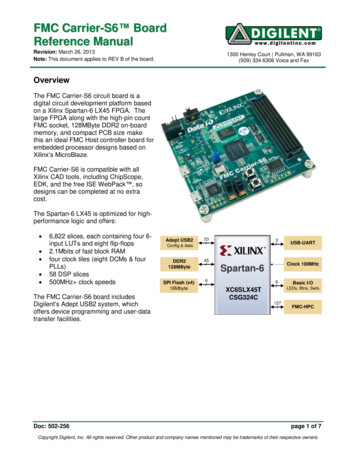
FMC Carrier-S6 BoardReference ManualRevision: March 26, 2013Note: This document applies to REV B of the board.1300 Henley Court Pullman, WA 99163(509) 334 6306 Voice and FaxOverviewThe FMC Carrier-S6 circuit board is adigital circuit development platform basedon a Xilinx Spartan-6 LX45 FPGA. Thelarge FPGA along with the high-pin countFMC socket, 128MByte DDR2 on-boardmemory, and compact PCB size makethis an ideal FMC Host controller board forembedded processor designs based onXilinx’s MicroBlaze.FMC Carrier-S6 is compatible with allXilinx CAD tools, including ChipScope,EDK, and the free ISE WebPack , sodesigns can be completed at no extracost.The Spartan-6 LX45 is optimized for highperformance logic and offers: 6,822 slices, each containing four 6input LUTs and eight flip-flops2.1Mbits of fast block RAMfour clock tiles (eight DCMs & fourPLLs)58 DSP slices500MHz clock speedsThe FMC Carrier-S6 board includesDigilent's Adept USB2 system, whichoffers device programming and user-datatransfer facilities.Doc: 502-256Adept USB2232Config & dataDDR2128MByte45SPI Flash (x4)16Mbyte6USB-UARTClock 100MHzSpartan-66Basic I/OLEDs, Btns, SwtsXC6SLX45TCSG324C127FMC-HPCpage 1 of 7Copyright Digilent, Inc. All rights reserved. Other product and company names mentioned may be trademarks of their respective owners.
FMC Carrier-S6 Reference ManualFeatures Xilinx Spartan-6 LX45 FPGA, 324-pin BGA package128Mbyte DDR2 with 16-bit wide dataon-board USB2 port for programming and data transferUSB-UART16Mbyte x4 SPI Flash for configuration and data storage100MHz OscillatorOver 120 GPIO signals available through FMC HPCGPIO includes 2 LEDs, 2 buttons, and 2 slide switchesships with 12V power supply and USB cableConfigurationAfter power-on, theFPGA on the FMCCarrier – S6 board mustbe configured (orprogrammed) before itcan perform anyfunctions. The FPGAcan be configured in twoways: a USBconnected PC canconfigure the boardusing the JTAG port anytime power is on and aconfiguration file storedin the SPI Flash ROMcan be automaticallytransferred to the FPGAat power-on.Adept USB PortJTAGPortUSBControllerJ2M0M1UART Port2SerialPort16Mbytes3V3Spartan-6FT232HQNumonyx SPIFlash (x4)SPIPortJP2Load to enableboot from ROMDoneJ3An on-board mode jumper (JP2) selects between JTAG/USB and ROM programming modes. If JP2 isloaded, the FPGA will automatically configure itself from the ROM. If JP2 is not loaded, the FPGA willremain idle after power-on until configured from the JTAG port.Both Digilent and Xilinx freely distribute software that can be used to program the FPGA and the SPIROM. Programming files are stored within the FPGA in SRAM-based memory cells. This data definesthe FPGA’s logic functions and circuit connections, and it remains valid until it is erased by removingpower or asserting the PROG B input, or until it is overwritten by a new configuration file.FPGA configuration files transferred via the JTAG port use the .bit or .svf file types. Xilinx’s ISEWebPack and EDK software can create .bit, .svf, .bin, or .mcs files from VHDL, Verilog, or schematicbased source files (EDK is used for MicroBlaze embedded processor-based designs).www.digilentinc.compage 2 of 7Copyright Digilent, Inc. All rights reserved. Other product and company names mentioned may be trademarks of their respective owners.
FMC Carrier-S6 Reference ManualAdept and iMPACT USB PortThe Adept port is compatible with Xilinx's iMPACT programming software if the Digilent Plug-In forXilinx Tools is installed on the host PC (download it free from the Digilent website’s software section).The plug-in automatically translates iMPACT-generated JTAG commands into formats compatiblewith the Digilent USB port, providing a seamless programming experience without leaving the Xilinxtool environment. Once the plug-in is installed, the "third party" programming option can be selectedfrom the iMPACT tools menu, and iMPACT will work as if a Xilinx programming cable were beingused. All Xilinx tools (iMPACT, ChipScope, EDK, etc.) can work with the plug-in, and they can beused in conjunction with Adept tools.Adept’s high-speed USB2 system can be used to program the FPGA and ROM and exchangeregister-based and file-based data with the FPGA. The Adept application, an SDK, and referencematerials are freely downloadable from the Digilent website.Power SuppliesThe FMC Carrier - S6 board requires an external 12V, 5A or greater power source with a coax centerpositive 2.1mm internal-diameter plug (a suitable supply is provided as a part of the FMC Carrier - S6kit). Voltage regulator circuits from Analog Devices create the required 3.3V, 1.8V, 1.23V and VADJsupplies from the main 12V supply. The table below provides additional information, typical currentsdepend strongly on FGPA configuration, and the values provided are typical of medium-size/speeddesigns).FMC Carrier - S6 Power SuppliesSupply12V3.3V1.8V1.23VVADJCircuitsFMC VCC12V0FPGA I/O, USB ports, clocks, ROMFPGA aux, GPIOFPGA core1V2, 1V8, 2V5, 3V3DeviceIC15: ADP1850IC15: ADP1850IC15: ADP1850IC23: LTC3546IC23: LTC3413Amps (max)5A4A1A3A4.2AA power-good LED (LD3), driven by the wired-OR of all the power-good outputs on the supplies,indicates that all supplies are operating within 10% of nominal.The VADJ rail has to be enabled by logic implemented in the FPGA. To do this, set the SET VADJ0and SET VADJ1 pins to indicate the desired voltage and drive VADJ EN high. It is important to notethat FPGA banks 0 and 1 are unpowered whenever VADJ EN is low. The table below outlines thedifferent voltages that may be selected:SET VADJ10011www.digilentinc.comFMC Carrier - S6 VADJ LevelsSET VADJ00101VADJ Voltage1.2V1.8V2.5V3.3Vpage 3 of 7Copyright Digilent, Inc. All rights reserved. Other product and company names mentioned may be trademarks of their respective owners.
FMC Carrier-S6 Reference ManualDDR2 MemoryA single 1Gbit DDR2 memory chip is driven from the memory controller block in the Spartan-6FGPA. The DDR2 device, a Micron MT47H64M16-25E or equivalent, provides a 16-bit bus and 64Mlocations. The FMC Carrier - S6 board has been tested for DDR2 operation at up to an 800MHz datarate.The DDR2 interface follows the pinout and routing guidelines specified in the Xilinx Memory InterfaceGenerator (MIG) User Guide. The interface supports SSTL18 signaling, and all address, data, clocks,and control signals are delay-matched and impedance-controlled. Address and control signals are notterminated. Two well-matched DDR2 clock signal pairs are provided so the DDR can be driven withlow-skew clocks from the DQS PUDQS NLDQS PLDQS NUDMLDMG3G1H7K6CKCK#CKEODTCS#Spartan-6See Tablewww.digilentinc.com13161V8VREFDDR2AddressA12: G6A4:A11: D3A3:A10: F4A2:A9: D1A1:A8: D2A0:A7: H6A6: H3A5: L2AD[12:0]DQ[15:0]page 4 of 7Copyright Digilent, Inc. All rights reserved. Other product and company names mentioned may be trademarks of their respective owners.
FMC Carrier-S6 Reference ManualFlash MemoryThe FMC Carrier - S6 board uses a 128Mbit NumonyxN25Q128 Serial Flash memory device (organized as 16-bitby 16Mbytes) for non-volatile storage of FPGAconfiguration files. The SPI Flash can be programmed witha .bit, .bin., or .mcs file using the Adept software. An FPGAconfiguration file requires less than 12Mbits, leaving116Mbits available for user data. Data can be transferredfrom a PC to/from the Flash by user applications, or byfacilities built into the Adept software. User designsprogrammed into the FPGA can also transfer data to andfrom the /DQ2HLD#/DQ3SCKSPI FlashA simple demo image has been loaded into the Serial Flash during manufacturing. It connects theUser LEDs (LD0, LD1) to the User Switches (SW0, SW1). The image along with the project source isavailable on the Digilent website.Oscillators/ClocksThe FMC Carrier - S6 board includes a single 100MHz Oscillator connected to pin T9 (T9 is a GCLKinput in bank 2). The input clock can drive any or all of the four clock management tiles in the Spartan6. Each tile includes two Digital Clock Managers (DCMs) and one Phase-Locked Loop (PLL).DCMs provide the four phases of the input frequency (0º, 90º, 180º, and 270º), a divided clock thatcan be the input clock divided by any integer from 2 to 16 or 1.5, 2.5, 3.5. 7.5, and two antiphaseclock outputs that can be multiplied by any integer from 2 to 32 and simultaneously divided by anyinteger from 1 to 32.PLLs use Voltage Controlled Oscillators (VCOs) that can be programmed to generate frequencies inthe 400MHz to 1080MHz range by setting three sets of programmable dividers during FPGAconfiguration. VCO outputs have eight equally-spaced outputs (0º, 45º, 90º, 135º, 180º, 225º, 270º,and 315º) that can be divided by any integer between 1 and 128.USB-UART Bridge (Serial Port)The FMC Carrier - S6 includes an FTDI USB-UART bridge to allow PC applications to communicatewith the board using a COM port. Free drivers allow COM-based (i.e., serial port) traffic on the PC tobe seamlessly transferred to the FMCCarrier – S6 board using the USBport at J3 marked UART. The FTDIT102TXDJ3part delivers the data to the SpartanRXDU10“UART”6 using a two-wire serial port withsoftware flow control (XON/XOFF).Micro-USBFT232HQSpartan-6Free Windows and Linux drivers canbe downloaded fromwww.ftdichip.com. After the drivers are installed, I/O commands from the PC directed to the COMport will produce serial data traffic on the T10 and Q10 FPGA pins.www.digilentinc.compage 5 of 7Copyright Digilent, Inc. All rights reserved. Other product and company names mentioned may be trademarks of their respective owners.
FMC Carrier-S6 Reference ManualBasic I/OThe FMC Carrier - S6 board includes two pushbuttons, two slide switches, and two LEDs for basicdigital input and output. The buttons and slide switches are connected to the FPGA via seriesresistors to prevent damage from inadvertent short circuits. The high efficiency LED anodes areconnected to the FPGA via 390-ohm resistors, and they will brightly illuminate with about 1mA ofcurrent when a logic high voltage is applied to their respective I/O pin.Pushbuttons10K10K10KPushbuttonsBTNU: E4BTND: F52Spartan-622Slide SwitchesSW0: U7SW1: V7LEDsLD0: V15LD1: N12390LEDsSlide SwitchesFMC-HPC ConnectorA single high-pin count (HPC) FMC slot is provided on the FMC Carrier – S6 to support a largeecosystem of plug-in modules. The FMC exposes 126 single-ended I/O, 102 of which can beconfigured as 51 differential pairs. The FMC interface spans over 4 PL I/O banks (banks 0, 1, 2, andMisc.). The FMC pin-out can be found in the FMC Carrier – S6 General UCF file.Quality AssuranceAll FMC Carrier - S6 boards are 100% tested during the manufacturing process. If any device on theFMC Carrier - S6 board fails test or is not responding properly, it is likely that damage occurred duringtransport or during use. Typical damage includes stressed solder joints and contaminants in switchesand buttons resulting in intermittent failures. Stressed solder joints can be repaired by reheating andreflowing solder and contaminants can be cleaned with off-the-shelf electronics cleaning products. If aboard fails test within the warranty period, it will be replaced at no cost. If a board fails test outside ofthe warranty period and cannot be easily repaired, Digilent can repair the board or offer a discountedreplacement. Contact Digilent for more details.www.digilentinc.compage 6 of 7Copyright Digilent, Inc. All rights reserved. Other product and company names mentioned may be trademarks of their respective owners.
FMC Carrier-S6 Reference ManualAppendix 1: Analog Devices ComponentsADG3308 – Low Voltage, 8-channel Bidirectional Logic Level Translatorshttp://www.analog.com/ADP3308ADG719 – CMOS MUX/SPDT Switchhttp://www.analog.com/ADG719ADP1850 – Dual DC-to-DC Synch Buck Controllerhttp://www.analog.com/ADP1850ADG804 – Low Voltage 4V, 4-Channel tinc.compage 7 of 7Copyright Digilent, Inc. All rights reserved. Other product and company names mentioned may be trademarks of their respective owners.
WebPack and EDK software can create .bit, .svf, .bin, or .mcs files from VHDL, Verilog, or schematic-based source files (EDK is used for MicroBlaze embedded processor-based designs). M0 M1 JTAG Port USB Controller Numonyx SPI Flash (x4) 16Mbytes SPI Port J2 Adept USB Port p art n-6 JP2 Done Load to enable b ot fr m ROM FT232HQ J3 UART Port .