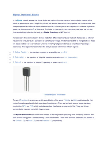
Transcription
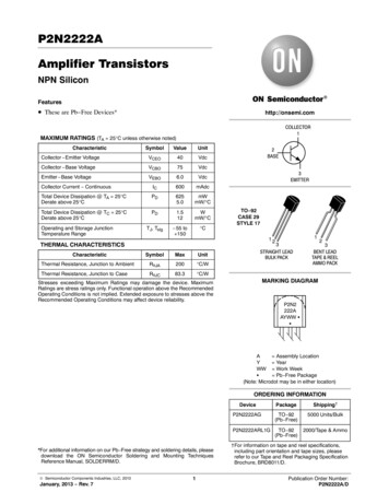
P2N2222AAmplifier TransistorsNPN SiliconFeatures These are Pb Free Devices*http://onsemi.comCOLLECTOR1MAXIMUM RATINGS (TA 25 C unless otherwise noted)CharacteristicSymbolValueUnitCollector Emitter VoltageVCEO40VdcCollector Base VoltageVCBO75VdcEmitter Base VoltageVEBO6.0VdcCollector Current ContinuousIC600mAdcTotal Device Dissipation @ TA 25 CDerate above 25 CPD6255.0mWmW/ CTotal Device Dissipation @ TC 25 CDerate above 25 CPD1.512WmW/ CTJ, Tstg 55 to 150 COperating and Storage JunctionTemperature Range2BASE3EMITTERTO 92CASE 29STYLE 17Characteristic112THERMAL CHARACTERISTICSSymbolMaxUnitThermal Resistance, Junction to AmbientRqJA200 C/WThermal Resistance, Junction to CaseRqJC83.3 C/W3STRAIGHT LEADBULK PACK23BENT LEADTAPE & REELAMMO PACKMARKING DIAGRAMStresses exceeding Maximum Ratings may damage the device. MaximumRatings are stress ratings only. Functional operation above the RecommendedOperating Conditions is not implied. Extended exposure to stresses above theRecommended Operating Conditions may affect device reliability.P2N2222AAYWW GGA Assembly LocationY YearWW Work WeekG Pb Free Package(Note: Microdot may be in either location)ORDERING INFORMATION*For additional information on our Pb Free strategy and soldering details, pleasedownload the ON Semiconductor Soldering and Mounting TechniquesReference Manual, SOLDERRM/D. Semiconductor Components Industries, LLC, 2013January, 2013 Rev. 71DevicePackageShipping†P2N2222AGTO 92(Pb Free)5000 Units/BulkP2N2222ARL1GTO 92(Pb Free)2000/Tape & Ammo†For information on tape and reel specifications,including part orientation and tape sizes, pleaserefer to our Tape and Reel Packaging SpecificationBrochure, BRD8011/D.Publication Order Number:P2N2222A/D
P2N2222AELECTRICAL CHARACTERISTICS (TA 25 C unless otherwise noted)CharacteristicSymbolMinMax40 UnitOFF CHARACTERISTICSCollector Emitter Breakdown Voltage(IC 10 mAdc, IB 0)V(BR)CEOCollector Base Breakdown Voltage(IC 10 mAdc, IE 0)V(BR)CBOEmitter Base Breakdown Voltage(IE 10 mAdc, IC 0)V(BR)EBOCollector Cutoff Current(VCE 60 Vdc, VEB(off) 3.0 Vdc)ICEXCollector Cutoff Current(VCB 60 Vdc, IE 0)(VCB 60 Vdc, IE 0, TA 150 C)ICBOEmitter Cutoff Current(VEB 3.0 Vdc, IC 0)IEBOCollector Cutoff Current(VCE 10 V)ICEOBase Cutoff Current(VCE 60 Vdc, VEB(off) 3.0 Vdc)IBEX75 6.0 10 0.0110 10 10 20355075351005040 300 0.31.00.6 1.22.0300 8.0 252.00.258.01.25 8.04.050753003755.02535200 150 4.0VdcVdcVdcnAdcmAdcnAdcnAdcnAdcON CHARACTERISTICSDC Current Gain(IC 0.1 mAdc, VCE 10 Vdc)(IC 1.0 mAdc, VCE 10 Vdc)(IC 10 mAdc, VCE 10 Vdc)(IC 10 mAdc, VCE 10 Vdc, TA 55 C)(IC 150 mAdc, VCE 10 Vdc) (Note 1)(IC 150 mAdc, VCE 1.0 Vdc) (Note 1)(IC 500 mAdc, VCE 10 Vdc) (Note 1)hFECollector Emitter Saturation Voltage (Note 1)(IC 150 mAdc, IB 15 mAdc)(IC 500 mAdc, IB 50 mAdc)VCE(sat)Base Emitter Saturation Voltage (Note 1)(IC 150 mAdc, IB 15 mAdc)(IC 500 mAdc, IB 50 mAdc)VBE(sat) VdcVdcSMALL SIGNAL CHARACTERISTICSCurrent Gain Bandwidth Product (Note 2)(IC 20 mAdc, VCE 20 Vdc, f 100 MHz)CfTOutput Capacitance(VCB 10 Vdc, IE 0, f 1.0 MHz)CoboInput Capacitance(VEB 0.5 Vdc, IC 0, f 1.0 MHz)CiboInput Impedance(IC 1.0 mAdc, VCE 10 Vdc, f 1.0 kHz)(IC 10 mAdc, VCE 10 Vdc, f 1.0 kHz)hieVoltage Feedback Ratio(IC 1.0 mAdc, VCE 10 Vdc, f 1.0 kHz)(IC 10 mAdc, VCE 10 Vdc, f 1.0 kHz)hreSmall Signal Current Gain(IC 1.0 mAdc, VCE 10 Vdc, f 1.0 kHz)(IC 10 mAdc, VCE 10 Vdc, f 1.0 kHz)hfeOutput Admittance(IC 1.0 mAdc, VCE 10 Vdc, f 1.0 kHz)(IC 10 mAdc, VCE 10 Vdc, f 1.0 kHz)hoeCollector Base Time Constant(IE 20 mAdc, VCB 20 Vdc, f 31.8 MHz)rb′CcNoise Figure(IC 100 mAdc, VCE 10 Vdc, RS 1.0 kW, f 1.0 kHz)NF1. Pulse Test: Pulse Width v 300 ms, Duty Cycle v 2.0%.2. fT is defined as the frequency at which hfe extrapolates to unity.http://onsemi.com2MHzpFpFkWX 10 4 mMhospsdB
P2N2222AELECTRICAL CHARACTERISTICS (TA 25 C unless otherwise noted) (Continued)CharacteristicSymbolMinMaxUnit(VCC 30 Vdc, VBE(off) 2.0 Vdc,IC 150 mAdc, IB1 15 mAdc) (Figure 1)td 10nstr 25ns(VCC 30 Vdc, IC 150 mAdc,IB1 IB2 15 mAdc) (Figure 2)ts 225nstf 60nsSWITCHING CHARACTERISTICSDelay TimeRise TimeStorage TimeFall TimeSWITCHING TIME EQUIVALENT TEST CIRCUITS 30 V 30 V1.0 to 100 ms,DUTY CYCLE 2.0% 16 V0- 2 V200 16 V1.0 to 100 ms,DUTY CYCLE 2.0%01 kW1k-14 VCS* 10 pF 2 ns 20 nsFigure 1. Turn On TimeCS* 10 pF1N914Scope rise time 4 ns*Total shunt capacitance of test jig,connectors, and oscilloscope.- 4 VFigure 2. Turn Off Time1000700500hFE, DC CURRENT GAIN200TJ 125 C30020025 C1007050-55 C30VCE 1.0 VVCE 10 V20100.10.20.30.5 0.71.02.03.05.0 7.0 1020 30IC, COLLECTOR CURRENT (mA)Figure 3. DC Current Gainhttp://onsemi.com35070100200300500 700 1.0 k
VCE , COLLECTOR-EMITTER VOLTAGE (VOLTS)P2N2222A1.0TJ 25 C0.80.6IC 1.0 mA10 mA150 mA500 mA0.40.200.0050.010.02 0.030.050.10.20.30.51.0IB, BASE CURRENT (mA)2.03.05.010203050Figure 4. Collector Saturation Region200500IC/IB 10TJ 25 Ctr @ VCC 30 Vtd @ VEB(off) 2.0 Vtd @ VEB(off) 03020107.05.0200t′s ts - 1/8 tf1007050tf3020107.05.03.02.05.0 7.01020 3050 70 100IC, COLLECTOR CURRENT (mA)200 3005005.0 7.0 10Figure 5. Turn On Time20030050010RS OPTIMUMRS SOURCERS RESISTANCEIC 1.0 mA, RS 150 W500 mA, RS 200 W100 mA, RS 2.0 kW50 mA, RS 4.0 kWf 1.0 kHz8.0NF, NOISE FIGURE (dB)NF, NOISE FIGURE (dB)6.020 3050 70 100IC, COLLECTOR CURRENT (mA)Figure 6. Turn Off Time108.0VCC 30 VIC/IB 10IB1 IB2TJ 25 C300t, TIME (ns)t, TIME (ns)10070504.02.0IC 50 mA100 mA500 mA1.0 mA6.04.02.000.01 0.02 0.05 0.1 0.20.5 1.0 2.05.0 102005050 100100 2005001.0 k 2.0 k5.0 k 10 k 20 kf, FREQUENCY (kHz)RS, SOURCE RESISTANCE (OHMS)Figure 7. Frequency EffectsFigure 8. Source Resistance Effectshttp://onsemi.com450 k 100 k
30CAPACITANCE (pF)20Ceb107.05.0Ccb3.02.00.10.2 0.30.5 0.7 1.02.0 3.0 5.0 7.0 10REVERSE VOLTAGE (VOLTS)20 3050f T, CURRENT-GAIN BANDWIDTH PRODUCT (MHz)P2N2222A500VCE 20 VTJ 25 C30020010070501.0Figure 9. Capacitances2.03.05.0 7.0 1020 30IC, COLLECTOR CURRENT (mA)5070 100Figure 10. Current Gain Bandwidth Product1.0 0.5TJ 25 C0COEFFICIENT (mV/ C)V, VOLTAGE (VOLTS)0.8VBE(sat) @ IC/IB 101.0 V0.6VBE(on) @ VCE 10 V0.40.2RqVC for VCE(sat)- 0.5- 1.0- 1.5RqVB for VBE- 2.0VCE(sat) @ IC/IB 100- 2.50.1 0.250 100 2000.5 1.0 2.0 5.0 10 20IC, COLLECTOR CURRENT (mA)500 1.0 k0.1 0.2Figure 11. “On” Voltages0.51.0 2.05.0 10 2050 100 200IC, COLLECTOR CURRENT (mA)Figure 12. Temperature Coefficientshttp://onsemi.com5500
MECHANICAL CASE OUTLINEPACKAGE DIMENSIONSTO 92 (TO 226)CASE 29 11ISSUE AMSCALE 1:11123STRAIGHT LEADBULK PACKDATE 09 MAR 200723BENT LEADTAPE & REELAMMO PACKABNOTES:1. DIMENSIONING AND TOLERANCING PER ANSIY14.5M, 1982.2. CONTROLLING DIMENSION: INCH.3. CONTOUR OF PACKAGE BEYOND DIMENSION RIS UNCONTROLLED.4. LEAD DIMENSION IS UNCONTROLLED IN P ANDBEYOND DIMENSION K MINIMUM.STRAIGHT LEADBULK PACKRPLSEATINGPLANEKDIMABCDGHJKLNPRVDX XGJHVCSECTION X OTES:1. DIMENSIONING AND TOLERANCING PERASME Y14.5M, 1994.2. CONTROLLING DIMENSION: MILLIMETERS.3. CONTOUR OF PACKAGE BEYONDDIMENSION R IS UNCONTROLLED.4. LEAD DIMENSION IS UNCONTROLLED IN PAND BEYOND DIMENSION K MINIMUM.BENT LEADTAPE & REELAMMO PACKBPTSEATINGPLANEGKDIMABCDGJKNPRVDX XJV1CNSECTION X --STYLES ON PAGE 2DOCUMENT NUMBER:STATUS:98ASB42022BON SEMICONDUCTOR STANDARDNEW STANDARD: Semiconductor Components Industries, LLC, 2002October, DESCRIPTION:2002 Rev. 0TO 92 (TO 226)http://onsemi.com1Electronic versions are uncontrolled except whenaccessed directly from the Document Repository. Printedversions are uncontrolled except when stamped“CONTROLLED COPY” in red.Case Outline Number:PAGE 1 OFXXX3
TO 92 (TO 226)CASE 29 11ISSUE AMDATE 09 MAR 2007STYLE 1:PIN 1. EMITTER2. BASE3. COLLECTORSTYLE 2:PIN 1. BASE2. EMITTER3. COLLECTORSTYLE 3:PIN 1. ANODE2. ANODE3. CATHODESTYLE 4:PIN 1. CATHODE2. CATHODE3. ANODESTYLE 5:PIN 1. DRAIN2. SOURCE3. GATESTYLE 6:PIN 1. GATE2. SOURCE & SUBSTRATE3. DRAINSTYLE 7:PIN 1. SOURCE2. DRAIN3. GATESTYLE 8:PIN 1. DRAIN2. GATE3. SOURCE & SUBSTRATESTYLE 9:PIN 1. BASE 12. EMITTER3. BASE 2STYLE 10:PIN 1. CATHODE2. GATE3. ANODESTYLE 11:PIN 1. ANODE2. CATHODE & ANODE3. CATHODESTYLE 12:PIN 1. MAIN TERMINAL 12. GATE3. MAIN TERMINAL 2STYLE 13:PIN 1. ANODE 12. GATE3. CATHODE 2STYLE 14:PIN 1. EMITTER2. COLLECTOR3. BASESTYLE 15:PIN 1. ANODE 12. CATHODE3. ANODE 2STYLE 16:PIN 1. ANODE2. GATE3. CATHODESTYLE 17:PIN 1. COLLECTOR2. BASE3. EMITTERSTYLE 18:PIN 1. ANODE2. CATHODE3. NOT CONNECTEDSTYLE 19:PIN 1. GATE2. ANODE3. CATHODESTYLE 20:PIN 1. NOT CONNECTED2. CATHODE3. ANODESTYLE 21:PIN 1. COLLECTOR2. EMITTER3. BASESTYLE 22:PIN 1. SOURCE2. GATE3. DRAINSTYLE 23:PIN 1. GATE2. SOURCE3. DRAINSTYLE 24:PIN 1. EMITTER2. COLLECTOR/ANODE3. CATHODESTYLE 25:PIN 1. MT 12. GATE3. MT 2STYLE 26:PIN 1. VCC2. GROUND 23. OUTPUTSTYLE 27:PIN 1. MT2. SUBSTRATE3. MTSTYLE 28:PIN 1. CATHODE2. ANODE3. GATESTYLE 29:PIN 1. NOT CONNECTED2. ANODE3. CATHODESTYLE 30:PIN 1. DRAIN2. GATE3. SOURCESTYLE 31:PIN 1. GATE2. DRAIN3. SOURCESTYLE 32:PIN 1. BASE2. COLLECTOR3. EMITTERSTYLE 33:PIN 1. RETURN2. INPUT3. OUTPUTSTYLE 34:PIN 1. INPUT2. GROUND3. LOGICSTYLE 35:PIN 1. GATE2. COLLECTOR3. EMITTERDOCUMENT NUMBER:STATUS:98ASB42022BON SEMICONDUCTOR STANDARDNEW STANDARD: Semiconductor Components Industries, LLC, 2002October, DESCRIPTION:2002 Rev. 0TO 92 (TO 226)http://onsemi.com2Electronic versions are uncontrolled except whenaccessed directly from the Document Repository. Printedversions are uncontrolled except when stamped“CONTROLLED COPY” in red.Case Outline Number:PAGE 2 OFXXX3
DOCUMENT NUMBER:98ASB42022BPAGE 3 OF 3ISSUEAMREVISIONADDED BENT LEAD TAPE & REEL VERSION. REQ. BY J. SUPINA.DATE09 MAR 2007ON Semiconductor andare registered trademarks of Semiconductor Components Industries, LLC (SCILLC). SCILLC reserves the right to make changes without further noticeto any products herein. SCILLC makes no warranty, representation or guarantee regarding the suitability of its products for any particular purpose, nor does SCILLC assume any liabilityarising out of the application or use of any product or circuit, and specifically disclaims any and all liability, including without limitation special, consequential or incidental damages.“Typical” parameters which may be provided in SCILLC data sheets and/or specifications can and do vary in different applications and actual performance may vary over time. Alloperating parameters, including “Typicals” must be validated for each customer application by customer’s technical experts. SCILLC does not convey any license under its patent rightsnor the rights of others. SCILLC products are not designed, intended, or authorized for use as components in systems intended for surgical implant into the body, or other applicationsintended to support or sustain life, or for any other application in which the failure of the SCILLC product could create a situation where personal injury or death may occur. ShouldBuyer purchase or use SCILLC products for any such unintended or unauthorized application, Buyer shall indemnify and hold SCILLC and its officers, employees, subsidiaries, affiliates,and distributors harmless against all claims, costs, damages, and expenses, and reasonable attorney fees arising out of, directly or indirectly, any claim of personal injury or deathassociated with such unintended or unauthorized use, even if such claim alleges that SCILLC was negligent regarding the design or manufacture of the part. SCILLC is an EqualOpportunity/Affirmative Action Employer. This literature is subject to all applicable copyright laws and is not for resale in any manner. Semiconductor Components Industries, LLC, 2007March, 2007 Rev. 11AMCase Outline Number:29
onsemi,, and other names, marks, and brands are registered and/or common law trademarks of Semiconductor Components Industries, LLC dba “onsemi” or its affiliatesand/or subsidiaries in the United States and/or other countries. onsemi owns the rights to a number of patents, trademarks, copyrights, trade secrets, and other intellectual property.A listing of onsemi’s product/patent coverage may be accessed at www.onsemi.com/site/pdf/Patent Marking.pdf. onsemi reserves the right to make changes at any time to anyproducts or information herein, without notice. The information herein is provided “as is” and onsemi makes no warranty, representation or guarantee regarding the accuracy of theinformation, product features, availability, functionality, or suitability of its products for any particular purpose, nor does onsemi assume any liability arising out of the application or useof any product or circuit, and specifically disclaims any and all liability, including without limitation special, consequential or incidental damages. Buyer is responsible for its productsand applications using onsemi products, including compliance with all laws, regulations and safety requirements or standards, regardless of any support or applications informationprovided by onsemi. “Typical” parameters which may be provided in onsemi data sheets and/or specifications can and do vary in different applications and actual performance mayvary over time. All operating parameters, including “Typicals” must be validated for each customer application by customer’s technical experts. onsemi does not convey any licenseunder any of its intellectual property rights nor the rights of others. onsemi products are not designed, intended, or authorized for use as a critical component in life support systemsor any FDA Class 3 medical devices or medical devices with a same or similar classification in a foreign jurisdiction or any devices intended for implantation in the human body. ShouldBuyer purchase or use onsemi products for any such unintended or unauthorized application, Buyer shall indemnify and hold onsemi and its officers, employees, subsidiaries, affiliates,and distributors harmless against all claims, costs, damages, and expenses, and reasonable attorney fees arising out of, directly or indirectly, any claim of personal injury or deathassociated with such unintended or unauthorized use, even if such claim alleges that onsemi was negligent regarding the design or manufacture of the part. onsemi is an EqualOpportunity/Affirmative Action Employer. This literature is subject to all applicable copyright laws and is not for resale in any manner.PUBLICATION ORDERING INFORMATIONLITERATURE FULFILLMENT:Email Requests to: orderlit@onsemi.comonsemi Website: www.onsemi.com TECHNICAL SUPPORTNorth American Technical Support:Voice Mail: 1 800 282 9855 Toll Free USA/CanadaPhone: 011 421 33 790 2910Europe, Middle East and Africa Technical Support:Phone: 00421 33 790 2910For additional information, please contact your local Sales Representative
y14.5m, 1982. 2. controlling dimension: inch. 3. contour of package beyond dimension r is uncontrolled. 4. lead dimension is uncontrolled in p and beyond dimension k minimum. r a p j l b k g h section x x v c d n n xx seating plane dim min max min max inches millimeters a 0.175 0.205 4.45 5