Transcription
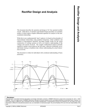
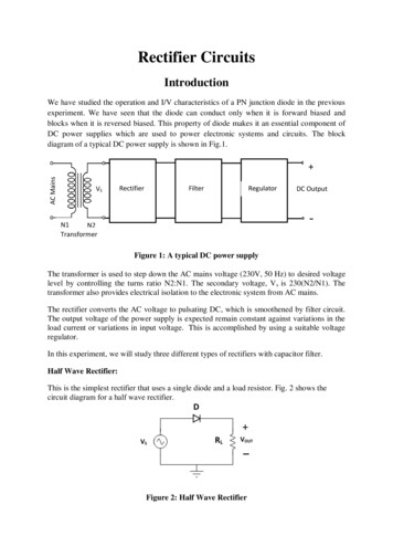
Rectifier CircuitsIntroductionWe have studied the operation and I/V characteristics of a PN junction diode in the previousexperiment. We have seen that the diode can conduct only when it is forward biased andblocks when it is reversed biased. This property of diode makes it an essential component ofDC power supplies which are used to power electronic systems and circuits. The blockdiagram of a typical DC power supply is shown in Fig.1.AC Mains VSRectifierFilterRegulatorDC Output-N1N2TransformerFigure 1: A typical DC power supplyThe transformer is used to step down the AC mains voltage (230V, 50 Hz) to desired voltagelevel by controlling the turns ratio N2:N1. The secondary voltage, V s is 230(N2/N1). Thetransformer also provides electrical isolation to the electronic system from AC mains.The rectifier converts the AC voltage to pulsating DC, which is smoothened by filter circuit.The output voltage of the power supply is expected remain constant against variations in theload current or variations in input voltage. This is accomplished by using a suitable voltageregulator.In this experiment, we will study three different types of rectifiers with capacitor filter.Half Wave Rectifier:This is the simplest rectifier that uses a single diode and a load resistor. Fig. 2 shows thecircuit diagram for a half wave rectifier.D VSRLVOUTFigure 2: Half Wave Rectifier
The diode is forward biased during each positive half cycle causing current to flow in thecircuit. These current results in voltage VOUT across the resistor RL. The waveform of VOUTwith respect to VS is shown in Fig.3.VoltageDC component of VOUTTimeVSVOUTThe output voltage is pulsating DC which has a significant AC component and DCcomponent which is the average value of VOUT. This kind of voltage is not suitable as a DCsupply. A simple way to make the output voltage smooth is to connect a filter capacitoracross the output terminals.VSCDuring positive half cycle as Vs increases, the diode D conducts allowing the capacitor tocharge to peak voltage of the sinusoid. After the peak, the voltage Vs starts decreasingmaking the anode of the diode at lesser voltage than cathode as the capacitor C holds thevoltage at cathode at the peak voltage. This reverse biases the diode D and the capacitor Cstarts discharging through RL till the voltage across (which is the voltage at the cathode) itbecomes less than Vs which is rising sinusoid. The diode then gets forward biased and startsconducting till the peak are reached and this cycle continues. The charging and discharging ofthe capacitor causes ripple voltage in the output. Larger capacitor (and /or RL) results inslower discharge and “flat” output giving rise to less ripple content.Ripple factor: Ripple factor is a measure of effectiveness of a rectifier circuit. It is defined asthe ratio of RMS value of the AC component (ripple component) Irrms in the outputwaveform to the DC component VDC in the output waveform.
r IrrmsI DCWe can measure the value of RMS component of overall output waveform from which wecan estimate the value of Irrms.We get,I rrms Irms 2 I DC2For half wave rectifier,I rms Im2I DC Im This leads to ripple factor r 1.21 for half wave rectifier.The ripple factor can be significantly reduced using a filter capacitor.For a half wave rectifier with filter capacitor, ripple factor is given by,1r 2 3 fR L CWhere f is the frequency of pulsating DC which in this case is same as that of AC mains.The value of ripple factor can also be estimated from the waveform of the output voltage.r Vrpp / 2 3V p 0.5VrppWhere Vp is the peak value of the output voltage and Vrpp is peak to peak value of the ripplevoltage.Filtered Output Voltage for C1 C2VoltageVpVrppFiltered Output Voltage for C2Time
Full wave rectifier with centretapped transformerThe circuit consists of a center-tapped transformer, followed by the rectifier formed by twodiodes D1 and D2, and finally the load R with a capacitor filter C. The circuit is designed suchthat the current through the load is always in the same direction during both the half cycles.Assume that the capacitor is not connected initially. Due to the center tap rectifier, during thepositive half cycle of the input Vs, A is positive with respect to B, hence diode D1 will beforward biased and D2 will be reverse biased. This results in the current flowing from A-D1R-B-A. In negative half cycle, C is positive with respect to B. This makes C positive withrespect to B causing diode D2 to get forward biased making the current flow from C-D2-RB-C. Thus in both the half cycles the current through R flows in the same direction resultingin pulsating DC across R.With capacitor filterDuring the positive half cycle, capacitor C will charge to the peak of the input waveformwhile the load R is being supplied current through D1. When the input starts to go below itspeak value, the voltage across C will cause D1 to be reverse biased, thus disconnecting therectifier from the load. The capacitor will then provide the necessary current for the load. Therate of potential drop across C will be based on the values of R & C.During the negative half cycle, diode D2 will initially be reverse biased due to voltage acrossC. When the voltage at the input crosses the dropping voltage across C, D2 will be forwardbiased. Now the load is supplied current by the input while simultaneously charging C. Thiscontinues till the negative peak of the input waveform, after which D2 will be reverse biased.The next positive cycle is similar to the previous negative cycle with diode D1 being forwardbiased when the input voltage crosses the voltage across C. Capacitor C ensures that thevoltage across load R remains close to the peak of the input voltage.
Bridge RectifierFig. 1 shows the circuit of diode bridge rectifier. The circuit uses four diodes D1, D2, D3 and D4connected in the form of bridge.During the positive cycle of Vs, point A is positive with respect to B causing diode D1 and D2 toforward bias and D3 and D4 to get reversed biased. This results in the current to flow from A, throughD1, R, D2, B to A.During negative cycle, the polarities change. Now point B is positive with respect to A causing diodesD3 and D4 to conduct and D1 and D2 to reverse bias. The resulting current then flows from B throughD4, R, D3, A to B. In both the cycles, the current through the load resistor R flows in the samedirection ensuring the pulsating DC across R in both the half cycles of the input voltage. Hence, this isa full wave rectifier.The output voltage can be smoothened by connecting a suitable capacitor across the load resistor asexplained in section B.Fig 2 shows the input output waveforms.Vm
The ripple factor of full wave rectifier (both centre tapped andbridge rectifier)The ripple factor is given by,r VrrmsVDC(1)where Vrrms is RMS value of AC component(ripple) in the rectifier output and VDC is the DCcomponent (average value) of the rectified output.Vrrms Vrms VDC22(2)where Vrms is the RMS value of the rectified output.For full wave rectifier,Vrms Vm2and V DC 2Vm (3)where, Vm is peak value of the voltage Vs. Substituting these values in (2) we get.r 0.483(4)This is a significant improvement in the ripple factor compared to that of a Half wave rectifier(r 1.21). However, this pulsating DC is not useful to power electronic circuits as it still has a largeAC component. The output can be made smooth by using capacitor filter as described in Half Waverectifier. Try to analyse the circuit in Fig. 3 and the waveforms in Fig 4.The ripple factor for full wave rectifier with capacitor filter is given by.r 14 3 fR L Cwhere f is the frequency of the signal Vs
Full wave rectifier with centretapped transformer The circuit consists of a center-tapped transformer, followed by the rectifier formed by two diodes D 1 and D2, and finally the load R with a capacitor filter C. The circuit is designed such that the current through the load is